8x8x8 LED Cube Driver
If you take a look back at the schematic you will see it is basically split in half. The right hand side is for the individual LED driver and the left side for Arduino and layer/cathode control. In this part of the hardware we're going to build up the right side of the schematic.
Building The Driver Circuit
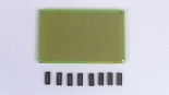
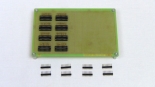
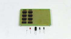
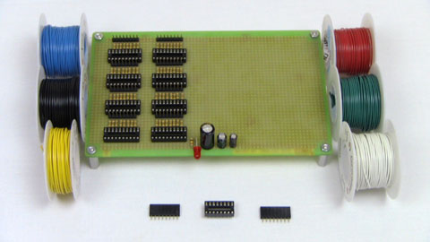
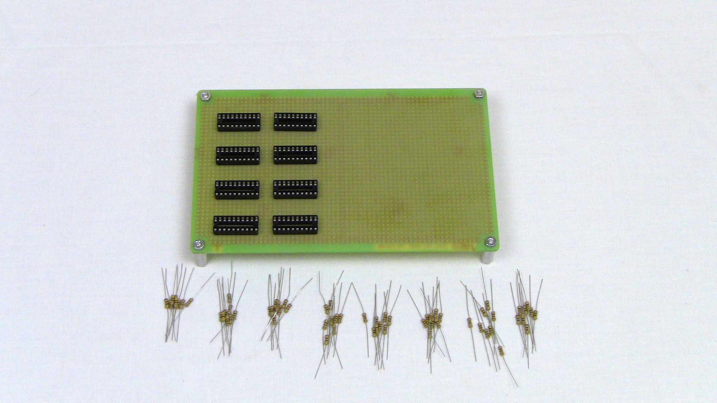
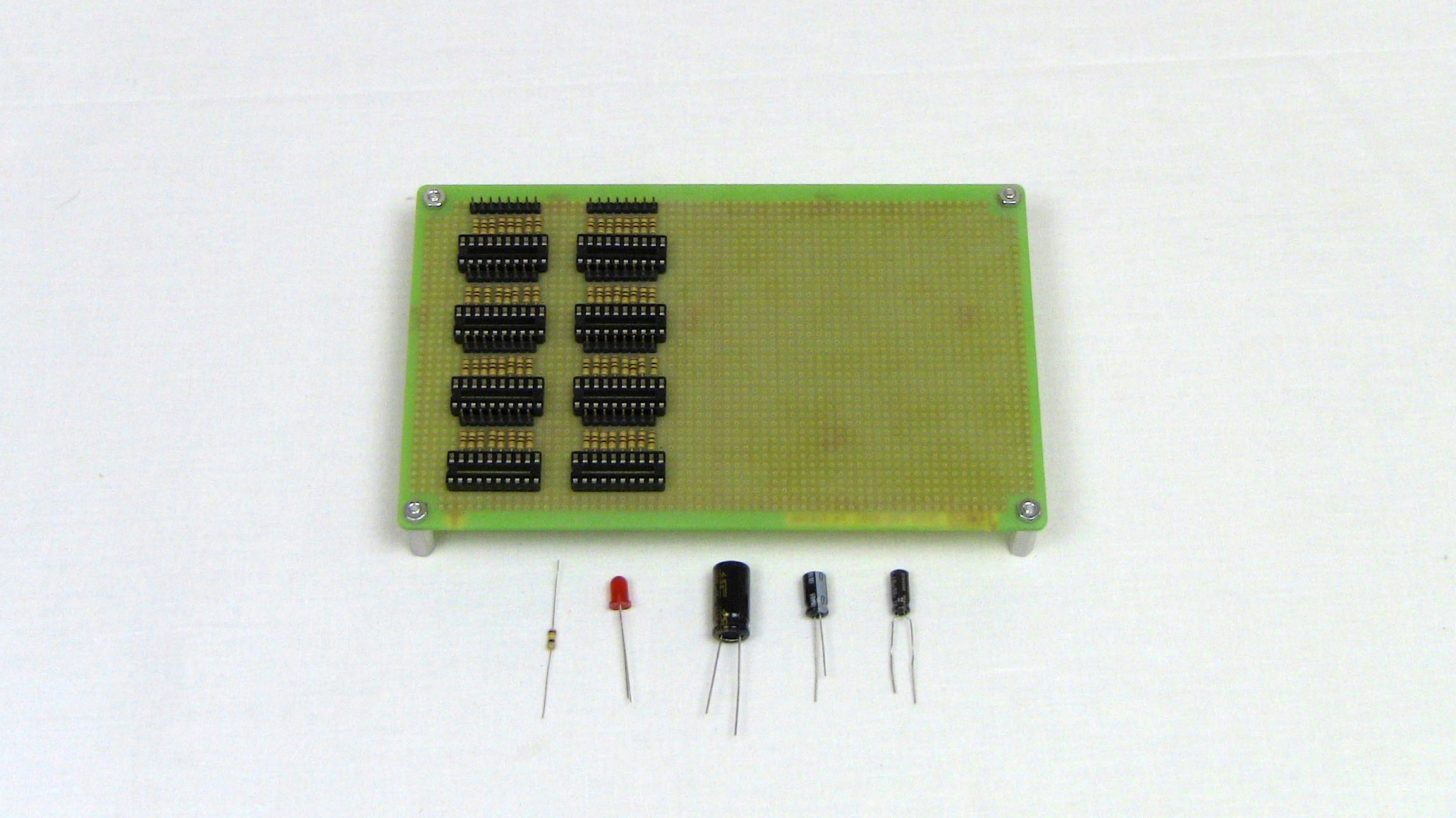
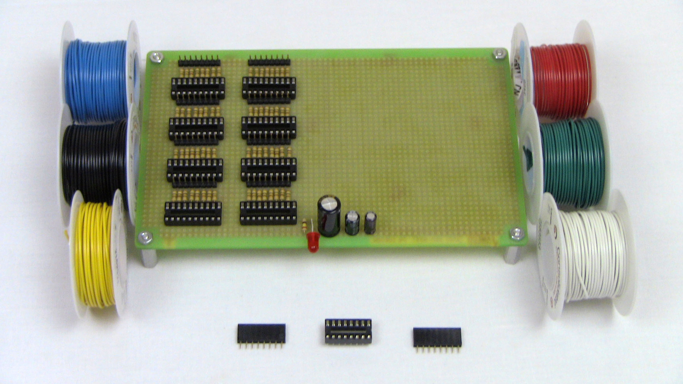
For the drive circuit we'll use half of the protoboard and save the other half for the arduino and cathode/layer control circuitry. To start, we'll need all the parts you see below:

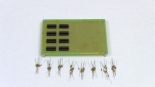
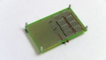
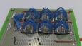
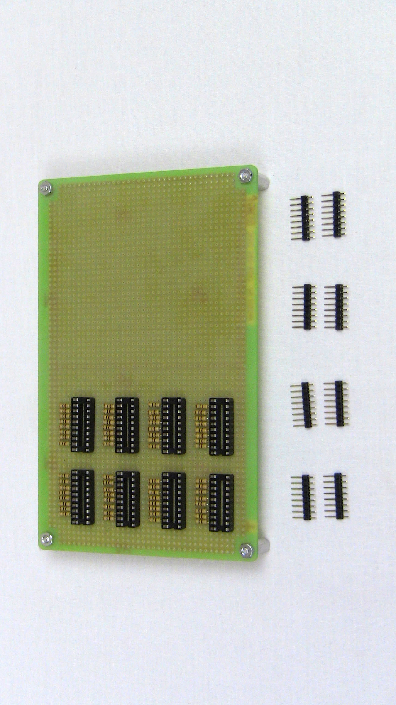
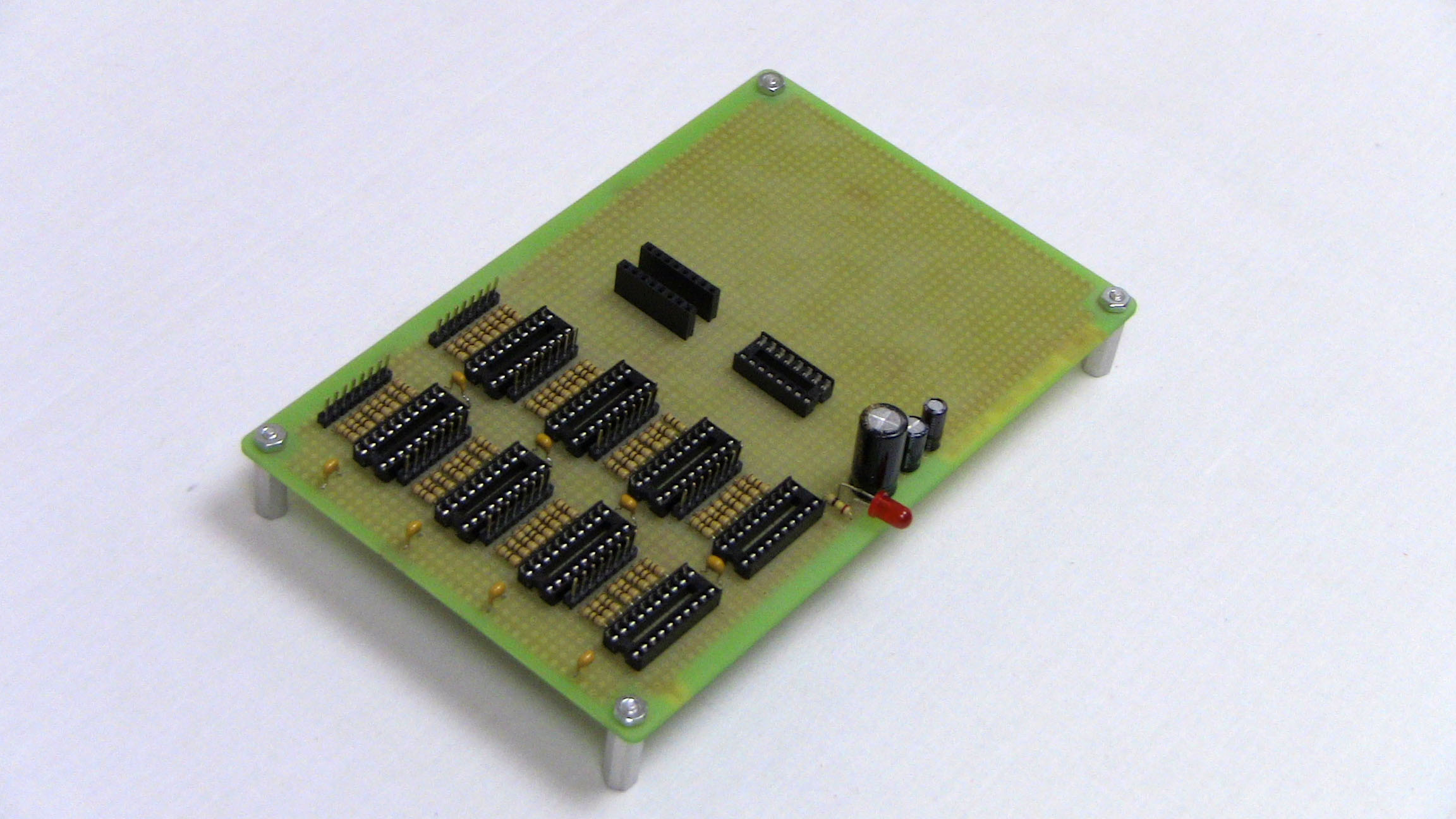
·First we need to figure out part placement for the 8 ICs. So we evenly organized them onto the protoboard with 5 holes of space between each other. Then 64 resistors fill in 4 holes of that spacing and an 8 pin header is inserted into the 5th hole. All of this makes it so that the original 5 hole spacing between 74HC574 IC's is filled in.
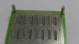
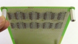
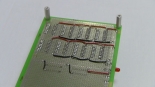
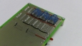
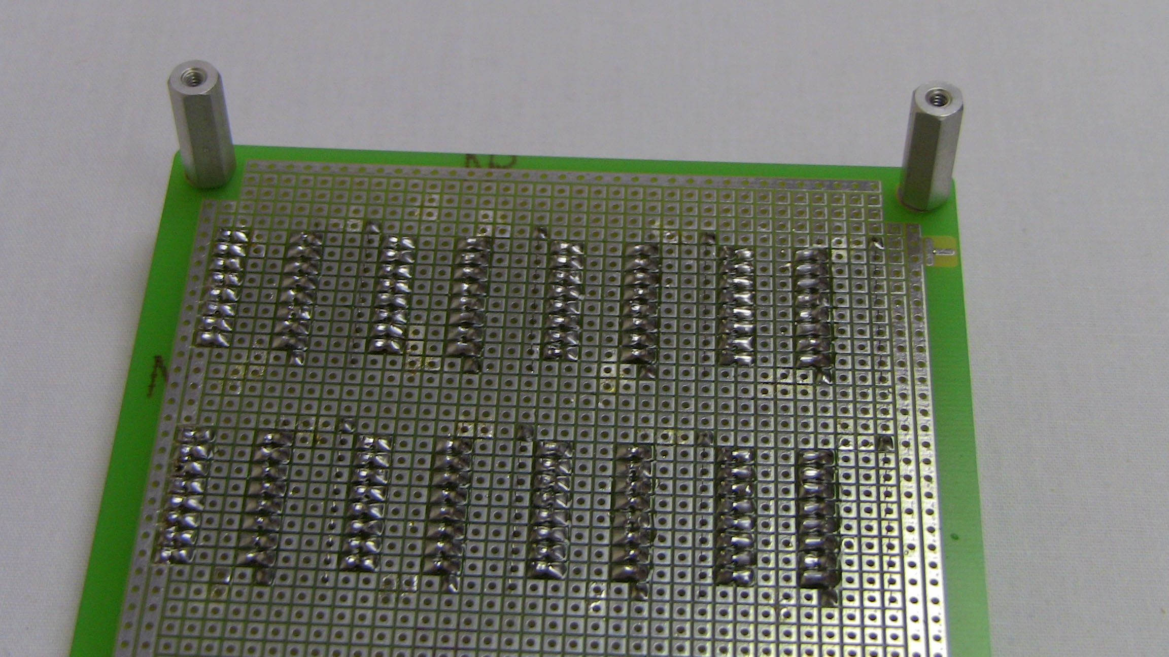
·Here are a few pictures of how we soldered the parts to the board. We did make a few mistakes, like how the IC on the left side of the board touches the bus line. So we used a razor blade and chopped the bus line into single pads like the rest of the board has.
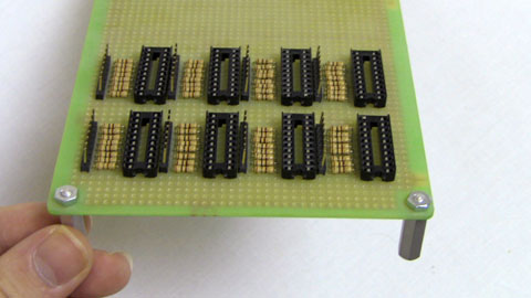
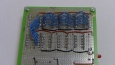
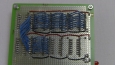
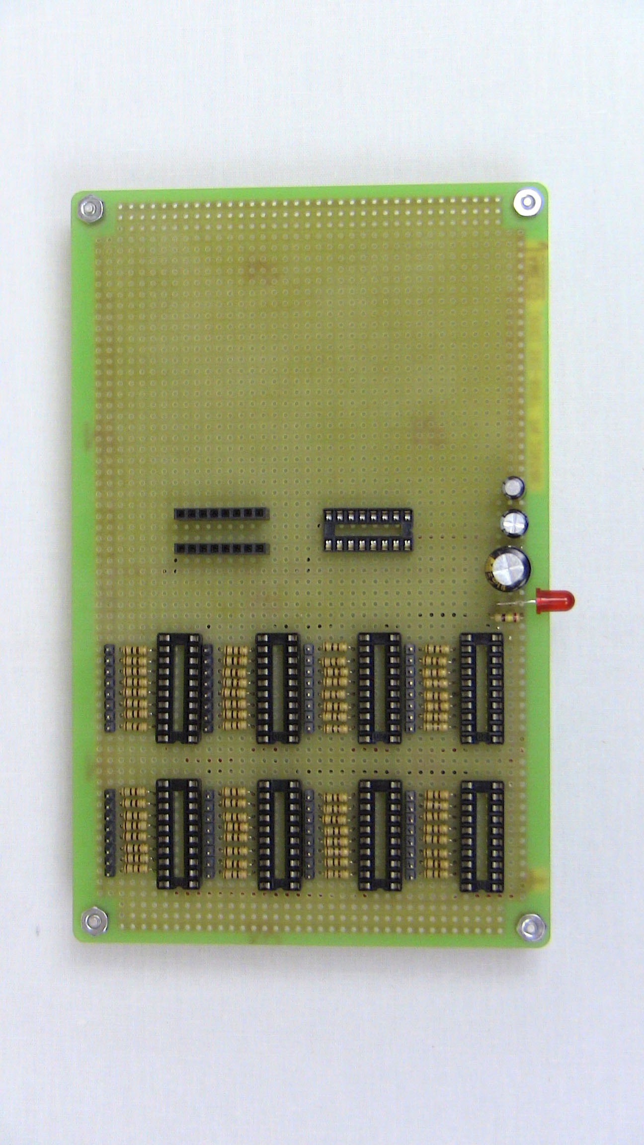
·After some soldering, here is the final part placement and layout for the 8 74HC574 ICs with their resistors and 8 pin headers.
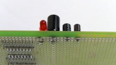
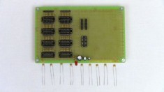
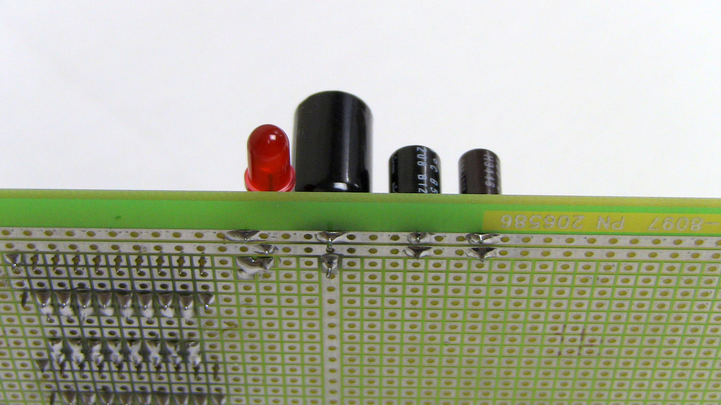
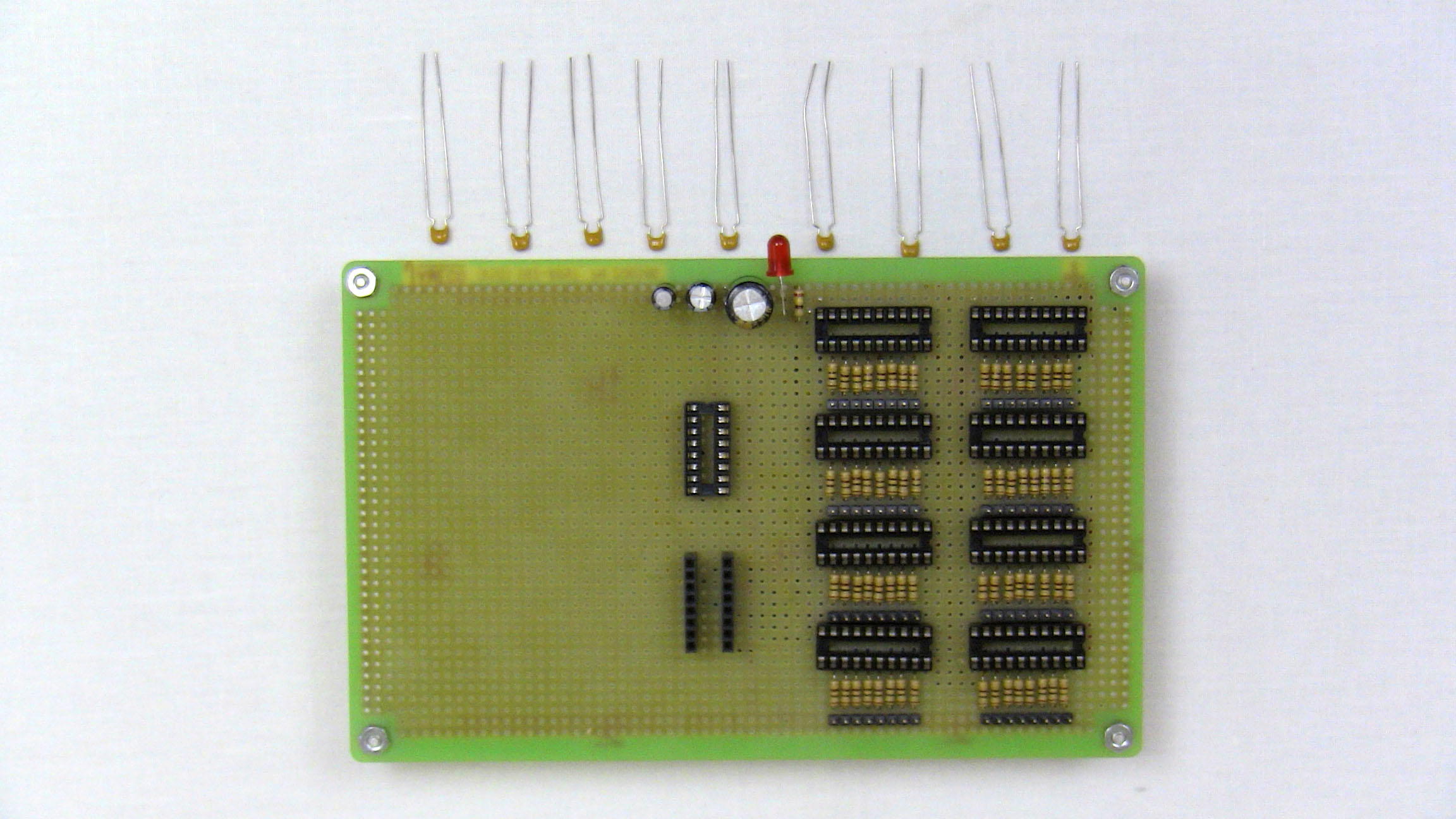
·Next we added the power circuitry that was a few capacitors 1000uF, 100uF and 10uF and a red led with a 240Ω current limiting resistor. These were all connected directly to the power and ground buses.
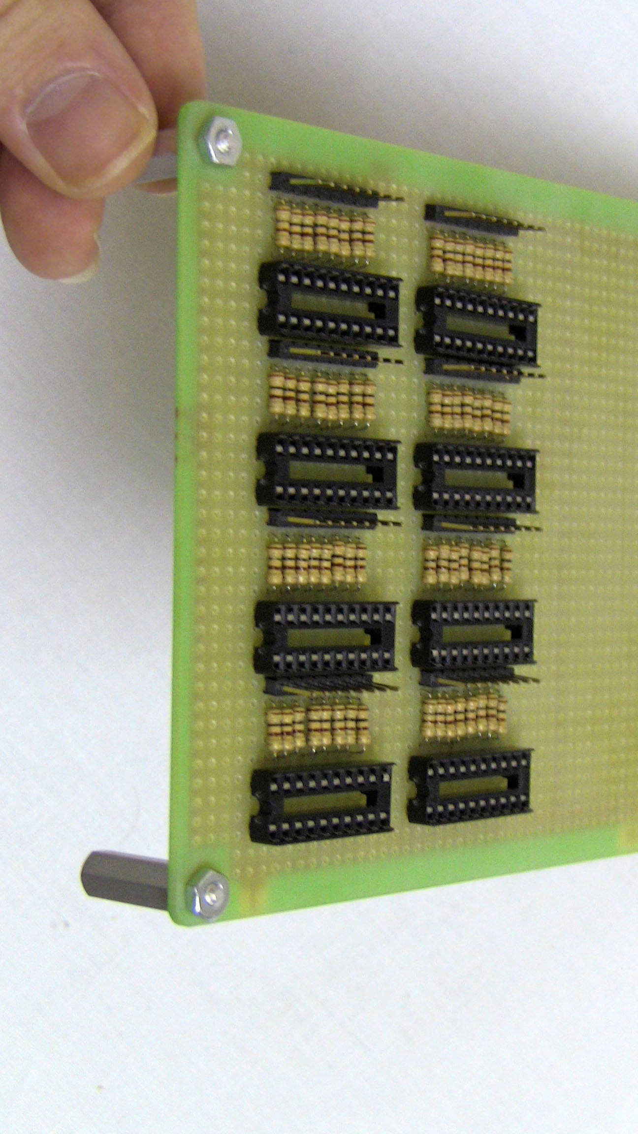
·The part placement to add is the 16 pin address decoder and J1(16 spot) connection port for the Arduino interface. The Address decoder is connected to all of the 74HC574's as well so we'll get started wiring everything together as well.
·So we placed and soldered down the 16 pin socket for the address decoder and J1 socket. We also connected all power and grounds using the red (+5v power) and black (ground) wire.
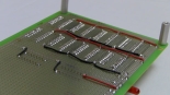
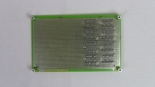
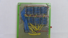
·At this point you should take a breather because the real work is about to begin. Here's the final part placement for the board:
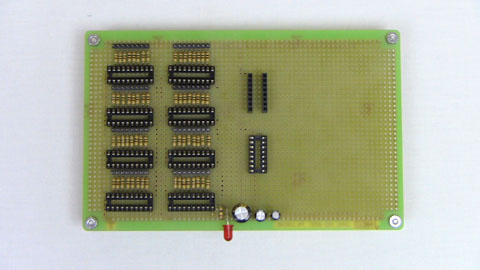
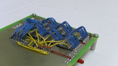
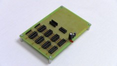
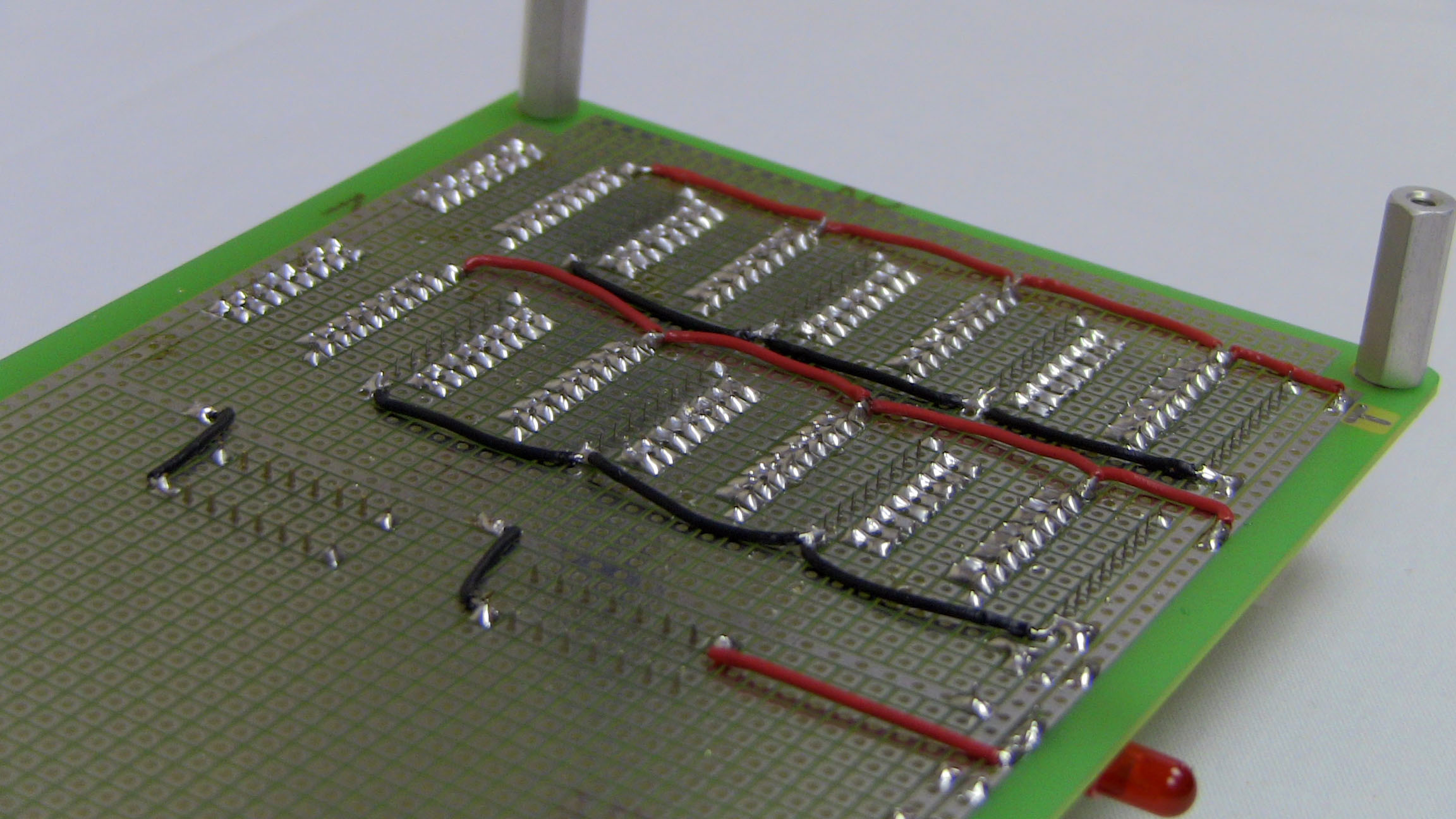
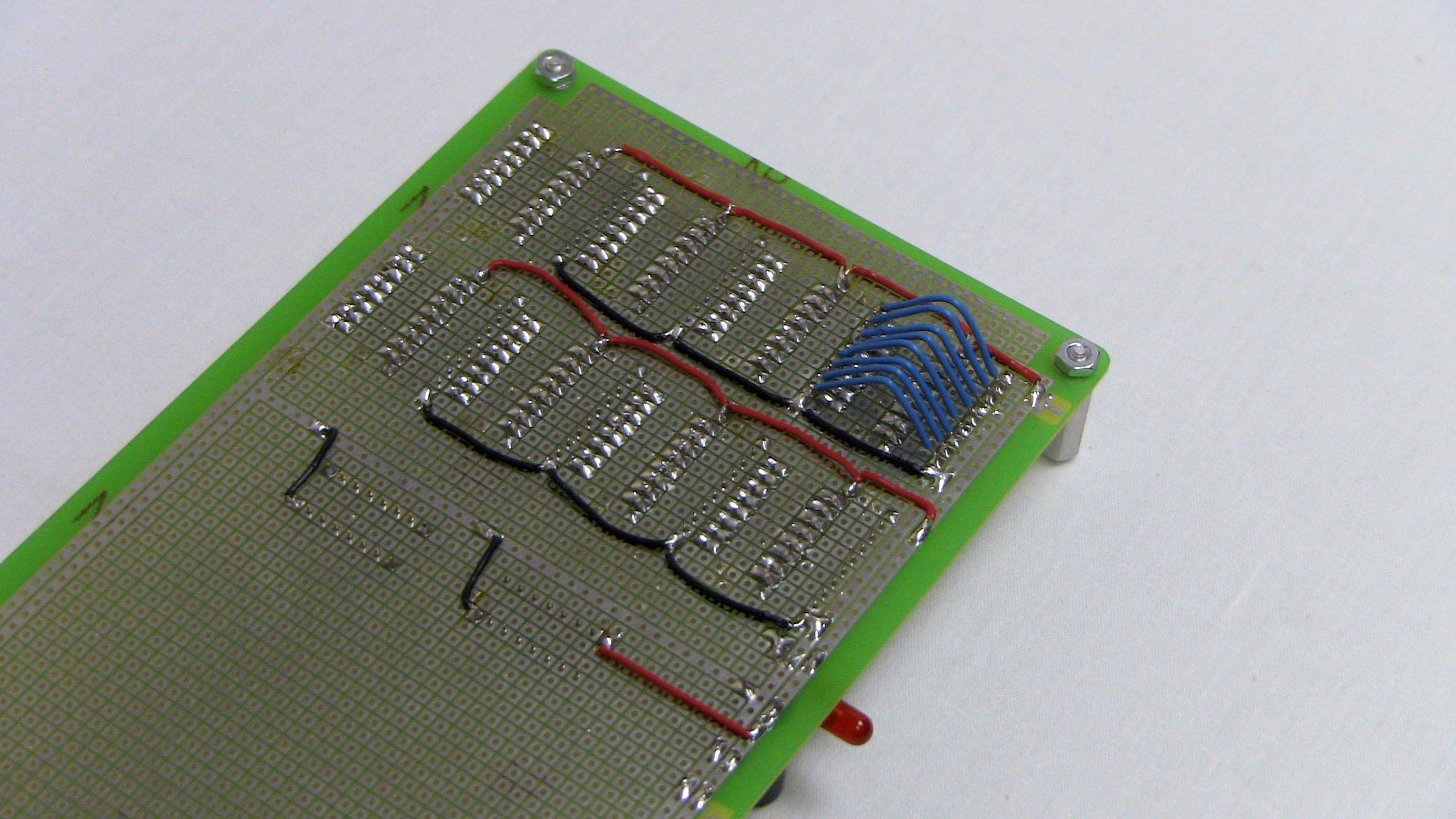
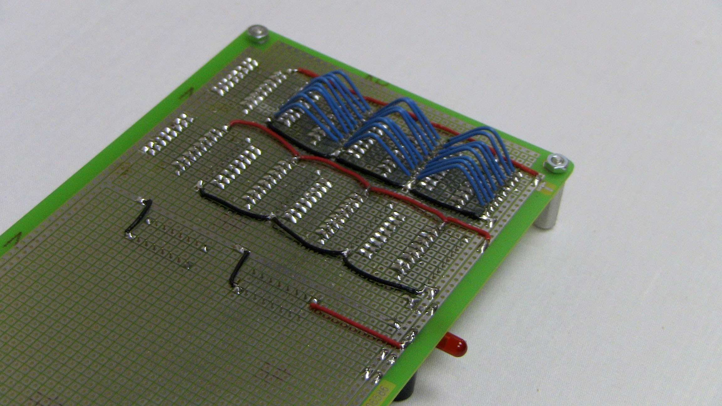
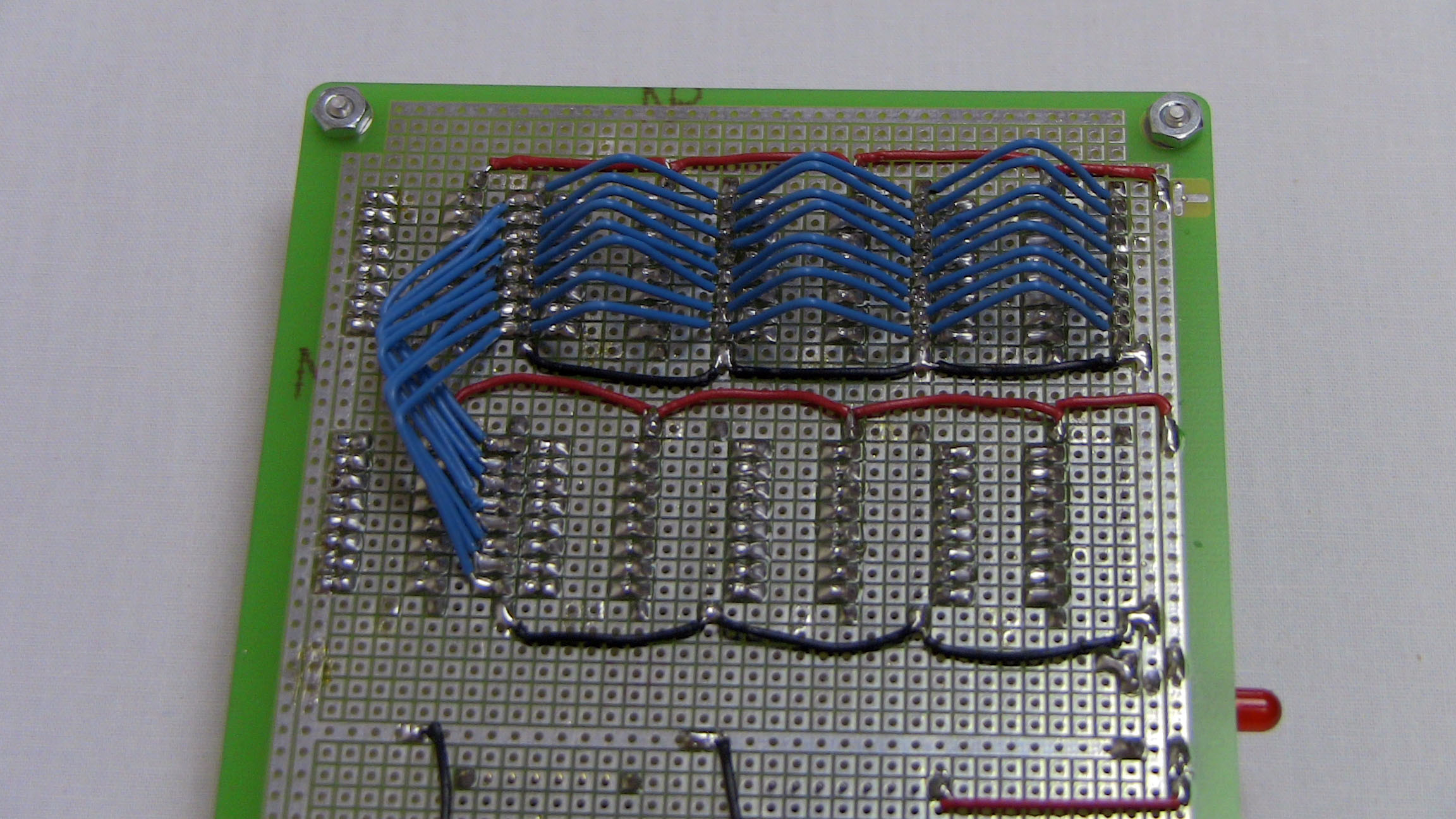
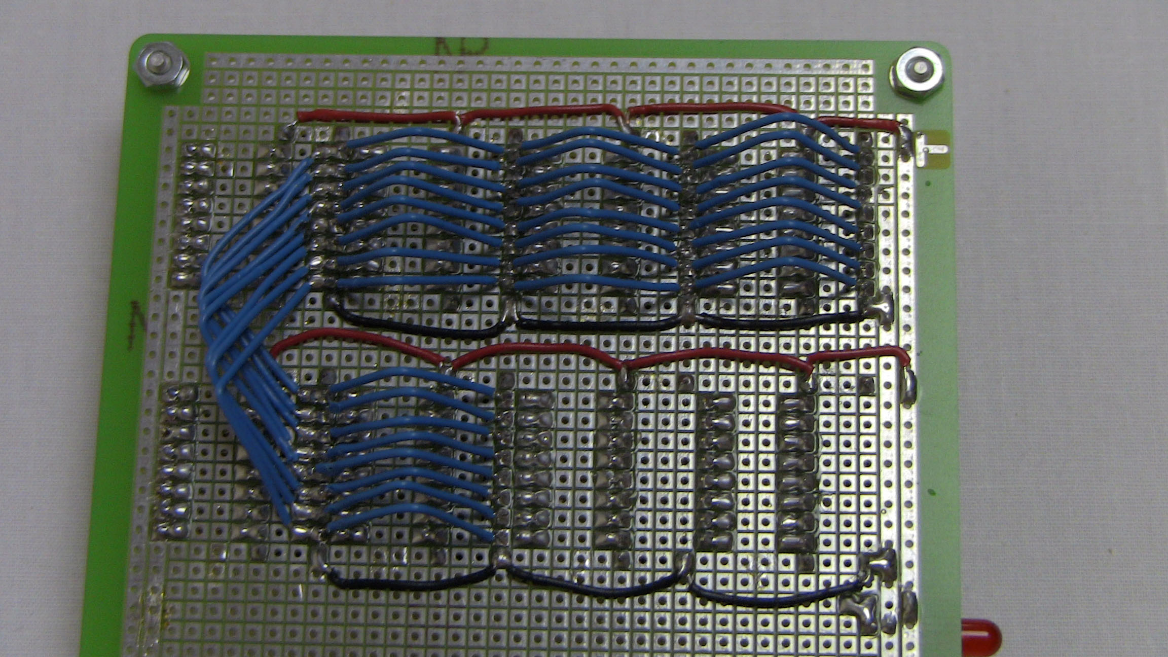
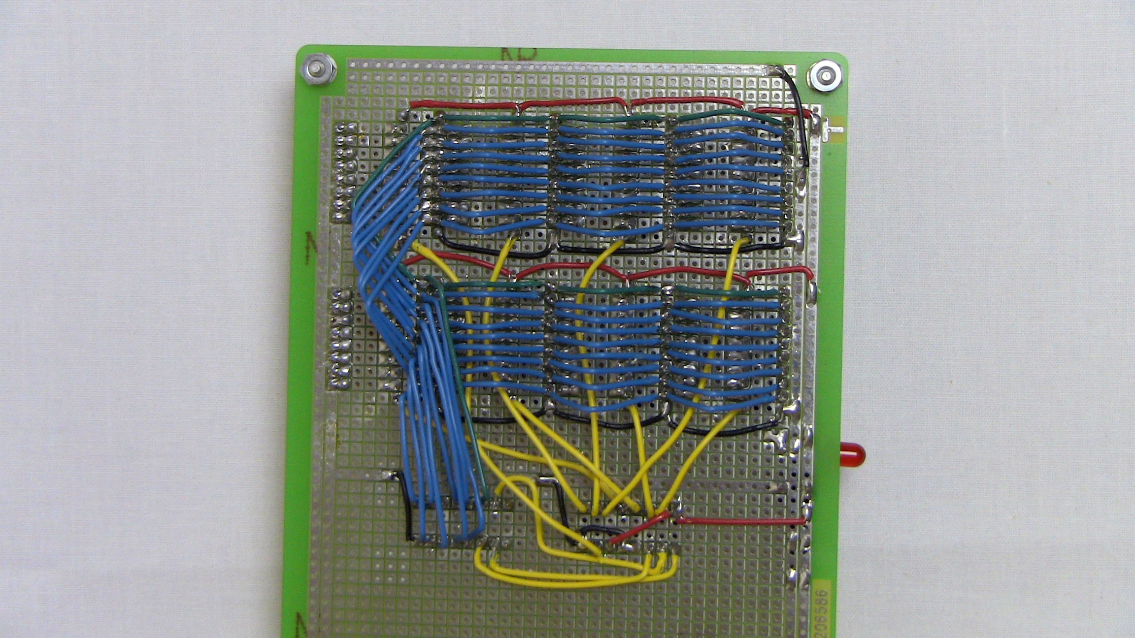
·Now we'll start connecting all of the D0, D1, D2, D3, D4, D5, D6 and D7 pins together on each of the 74HC574 IC's. This takes a while. We used blue wire for this data bus.

·We decided to use a triangle connect method as you can see. We think it makes the connections more obvious for people trying to understand how it's all connected together. Anyway, one at a time, connect all the D0's together and D1's...and etc.
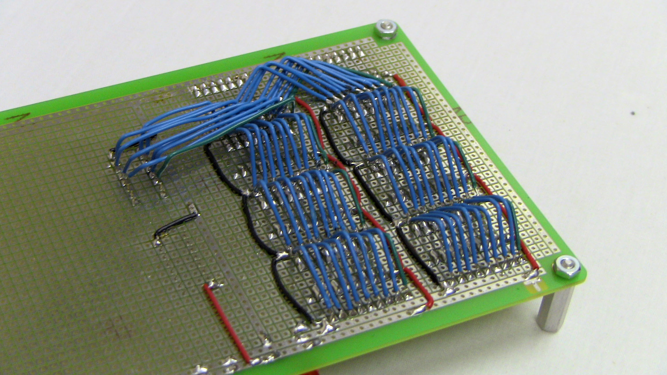
·Now, connect all of the output control pins together as well (teal wire along side the data bus) and then connect them all over to the J1 connector.

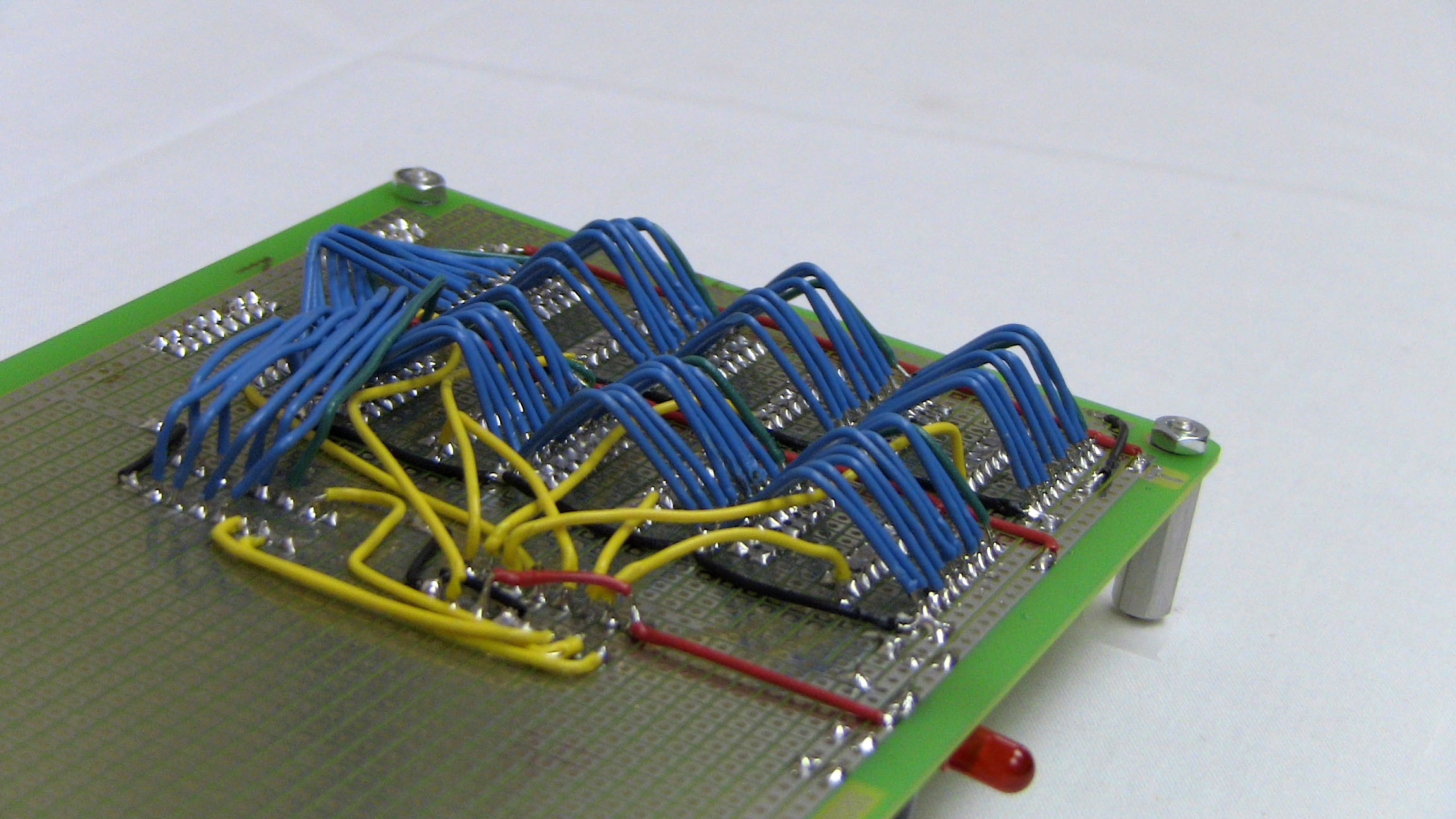
·Using yellow wire for the address decoder, we connected all of the clock pins from the 74HC574's sockets to each of the output pins for the 74HC138's socket. And then the control pins 1,2 and 3 were connected with yellow wire to the arduino interface connector J1.
·The last step for this side of the schematic is to add some DC coupling capacitors near the 74HC574's. This is to improve switching performance. Not a big deal, but they are important!
·Well, now we're half done with building the circuit. No sweat right? Right....anyway let's continue on to build the rest of the Arduino interface and the cathode control.
If you take a look back at the schematic you will see it is basically split in half. The right hand side is for the individual LED driver and the left side for Arduino and layer/cathode control. In this part of the hardware we're going to build up the right side of the schematic.
Building The Driver Circuit
For the drive circuit we'll use half of the protoboard and save the other half for the arduino and cathode/layer control circuitry. To start, we'll need all the parts you see below:

·First we need to figure out part placement for the 8 ICs. So we evenly organized them onto the protoboard with 5 holes of space between each other. Then 64 resistors fill in 4 holes of that spacing and an 8 pin header is inserted into the 5th hole. All of this makes it so that the original 5 hole spacing between 74HC574 IC's is filled in.

·Here are a few pictures of how we soldered the parts to the board. We did make a few mistakes, like how the IC on the left side of the board touches the bus line. So we used a razor blade and chopped the bus line into single pads like the rest of the board has.

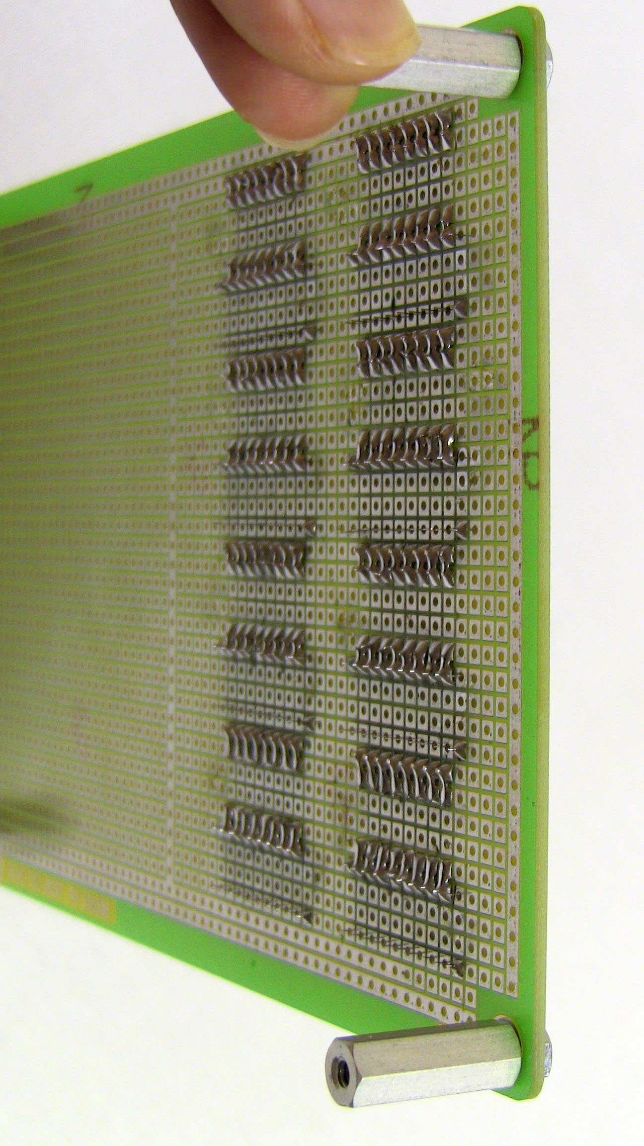
·After some soldering, here is the final part placement and layout for the 8 74HC574 ICs with their resistors and 8 pin headers.
·Next we added the power circuitry that was a few capacitors 1000uF, 100uF and 10uF and a red led with a 240Ω current limiting resistor. These were all connected directly to the power and ground buses.
·The part placement to add is the 16 pin address decoder and J1(16 spot) connection port for the Arduino interface. The Address decoder is connected to all of the 74HC574's as well so we'll get started wiring everything together as well.
·So we placed and soldered down the 16 pin socket for the address decoder and J1 socket. We also connected all power and grounds using the red (+5v power) and black (ground) wire.
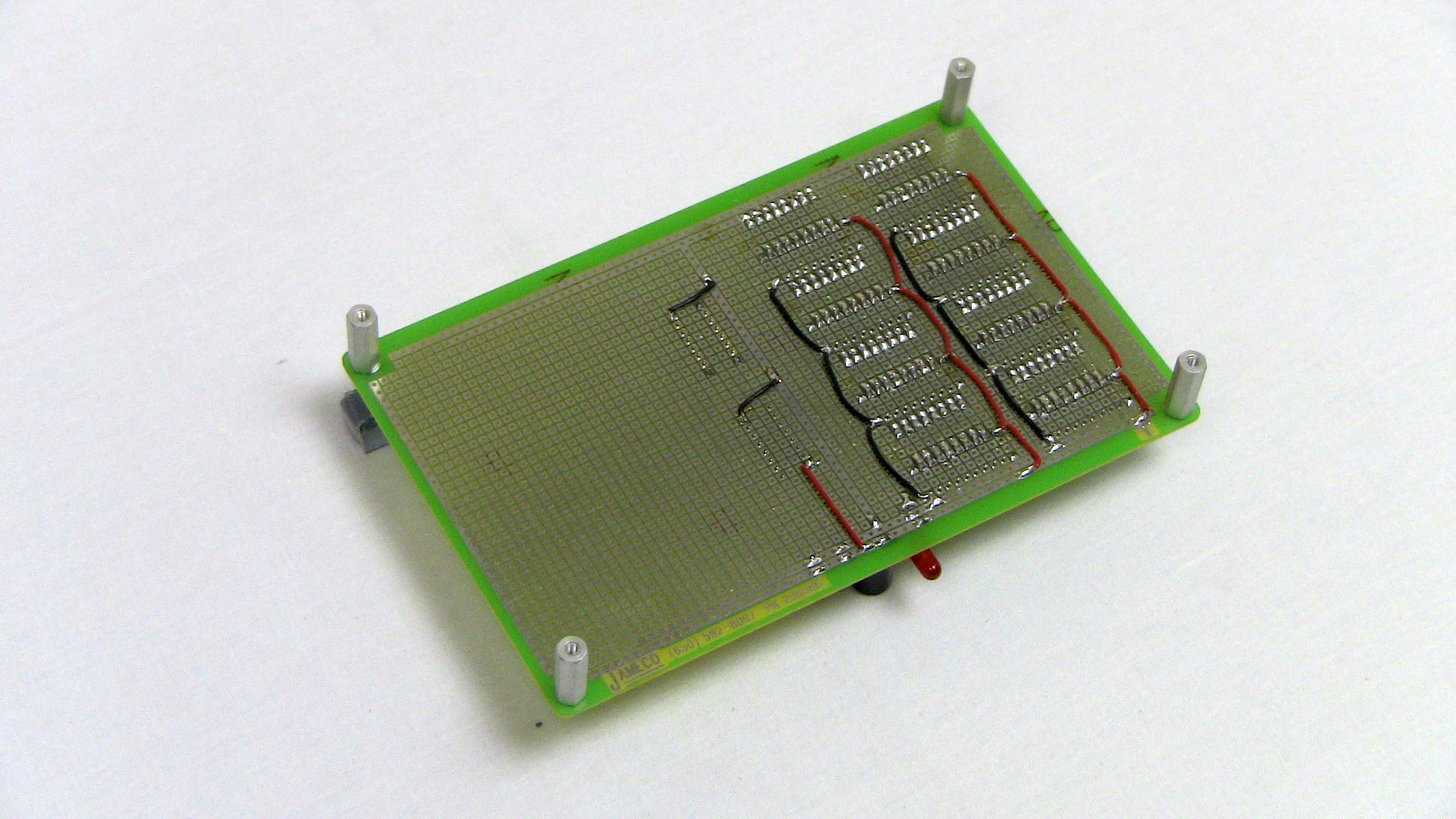

·At this point you should take a breather because the real work is about to begin. Here's the final part placement for the board:
·Now we'll start connecting all of the D0, D1, D2, D3, D4, D5, D6 and D7 pins together on each of the 74HC574 IC's. This takes a while. We used blue wire for this data bus.
·We decided to use a triangle connect method as you can see. We think it makes the connections more obvious for people trying to understand how it's all connected together. Anyway, one at a time, connect all the D0's together and D1's...and etc.

·Now, connect all of the output control pins together as well (teal wire along side the data bus) and then connect them all over to the J1 connector.
·Using yellow wire for the address decoder, we connected all of the clock pins from the 74HC574's sockets to each of the output pins for the 74HC138's socket. And then the control pins 1,2 and 3 were connected with yellow wire to the arduino interface connector J1.
·The last step for this side of the schematic is to add some DC coupling capacitors near the 74HC574's. This is to improve switching performance. Not a big deal, but they are important!
·Well, now we're half done with building the circuit. No sweat right? Right....anyway let's continue on to build the rest of the Arduino interface and the cathode control.