Hardware Design
This hardware section will show you the exact hardware changes that were made to modify the standard CPLD Dev Board so that it could be used as an A/D Converter + LED Output interface.
Building The Complex Circuit
The first two pictures show the CPLD Dev Board as we left it at the end of the tutorial.
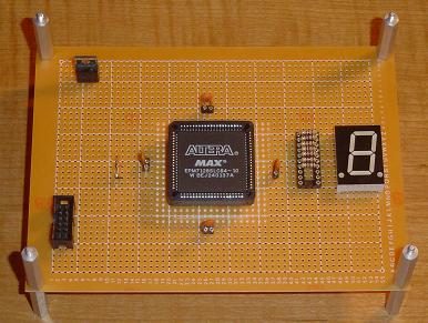
·Above: The Top of the Dev Board, Below: The Bottom Side
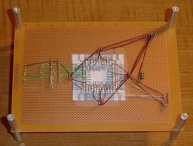
·Following the schematic, you can see the next hardware additions:

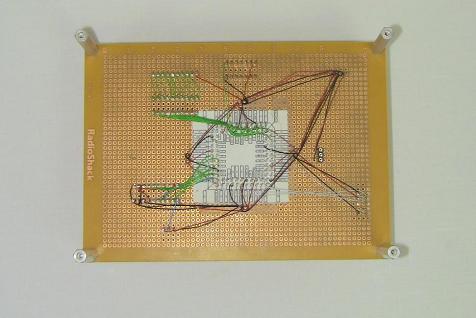
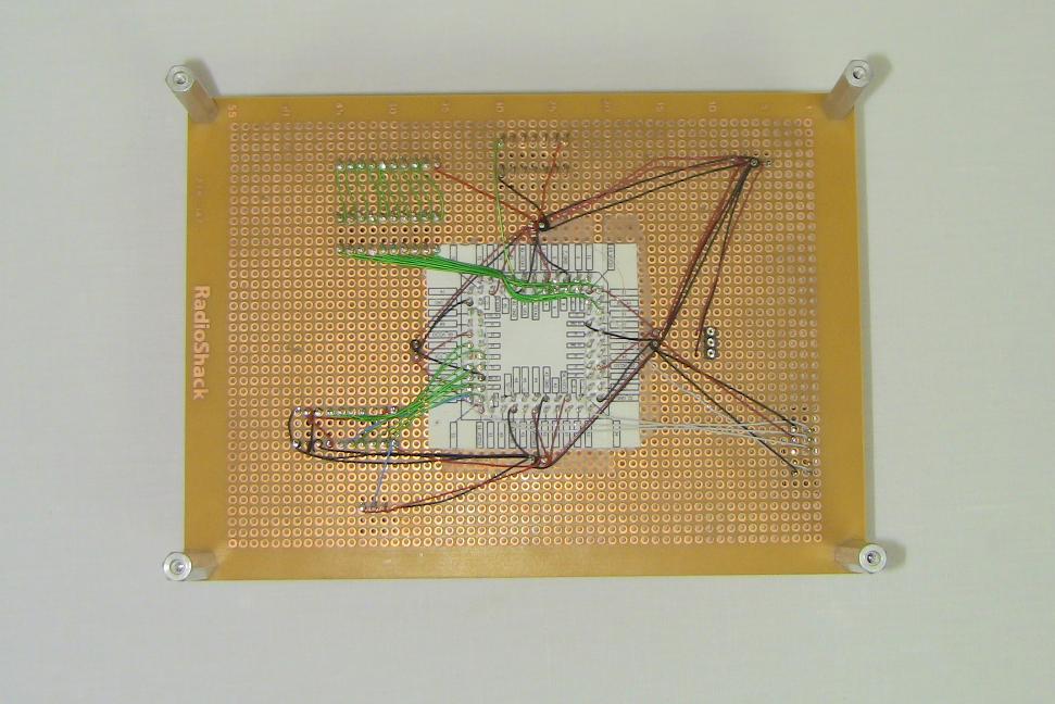
·Using wire wrap, all the connections from the schematic are made:
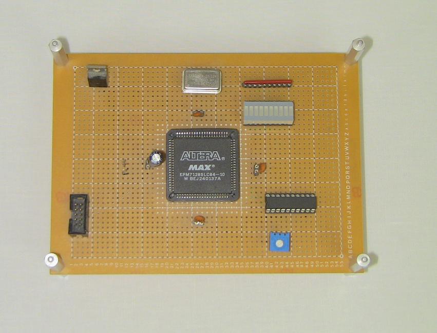
·After the wire-wrapping is complete, we're ready to load in the configuration!
This hardware section will show you the exact hardware changes that were made to modify the standard CPLD Dev Board so that it could be used as an A/D Converter + LED Output interface.
Building The Complex Circuit
The first two pictures show the CPLD Dev Board as we left it at the end of the tutorial.
·Above: The Top of the Dev Board, Below: The Bottom Side
·Following the schematic, you can see the next hardware additions:
·Using wire wrap, all the connections from the schematic are made:
·After the wire-wrapping is complete, we're ready to load in the configuration!