Schematic Overview
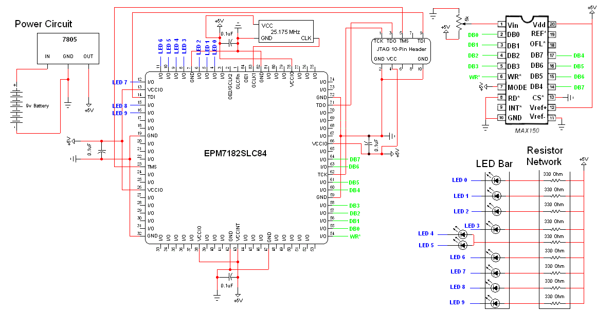
The schematic for this project is meant to be as simple as possible. We will be using the same CPLD setup from the standard CPLD Dev Board with a few additions. In addition to the EPM7128 CPLD, a new MAX150, 330Ω Resistor Network and LED Bar will be added.

View Large Schematic
Schematic Specifics
CPLD Dev Board Basics
The basic connections on the standard CPLD board are the JTAG connection, Power Supply and 25.175 MHz Oscillator.
Resistor Network + LED Bar
The LED bar has 10 LEDs, however our resistor network only has 9 resistor spots, so 1 of those resistors will be connected to the two middle LEDs on the LED bar so we can control all the LEDs, not just 9.
MAX150 Circuit
The MAX150 will be configured for WR mode, but connecting power and ground to the MODE/CS pins. The DB0-DB7 (Data Bit) pins are all connected to the FPGA and the WR* is connected as well. WR* will be pulsed by the FPGA to tell the MAX150 to update the data output.
The schematic for this project is meant to be as simple as possible. We will be using the same CPLD setup from the standard CPLD Dev Board with a few additions. In addition to the EPM7128 CPLD, a new MAX150, 330Ω Resistor Network and LED Bar will be added.
View Large Schematic
Schematic Specifics
CPLD Dev Board Basics
The basic connections on the standard CPLD board are the JTAG connection, Power Supply and 25.175 MHz Oscillator.
Resistor Network + LED Bar
The LED bar has 10 LEDs, however our resistor network only has 9 resistor spots, so 1 of those resistors will be connected to the two middle LEDs on the LED bar so we can control all the LEDs, not just 9.
MAX150 Circuit
The MAX150 will be configured for WR mode, but connecting power and ground to the MODE/CS pins. The DB0-DB7 (Data Bit) pins are all connected to the FPGA and the WR* is connected as well. WR* will be pulsed by the FPGA to tell the MAX150 to update the data output.