MAX150 Interface
Since we wired up the MAX150 to WR mode, we only have to send a single pulse to the WR pin to tell the A/D to start a conversion. The process from power up to displaying the digital output on the LEDs can be seen in the simplified float chart below:
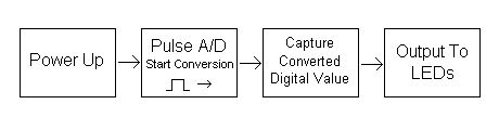
After the LEDs have been updated with the most current A/D conversion value, the process starts over again, pulsing the A/D to convert, then getting the new value and updating the LEDs, until infinity.
Analog To Digital
The MAX150 takes in an analog voltage between two reference voltages. Then this value is converted to a magnitude value in an 8 bit digital format. The chart belows gives one example for how to calculate what digital value to expect, given a specific analog voltage input.
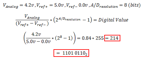
The two reference voltages seen above, Vref+ and Vref- are the same as we'll be using for this project, +5.0v and +0.0v respectively. So you can plug in any analog voltages to the formula and see what the digital equivalent will turn out to be. Then after building this project you can verify that your system is working correctly with this theory.
Since we wired up the MAX150 to WR mode, we only have to send a single pulse to the WR pin to tell the A/D to start a conversion. The process from power up to displaying the digital output on the LEDs can be seen in the simplified float chart below:
After the LEDs have been updated with the most current A/D conversion value, the process starts over again, pulsing the A/D to convert, then getting the new value and updating the LEDs, until infinity.
Analog To Digital
The MAX150 takes in an analog voltage between two reference voltages. Then this value is converted to a magnitude value in an 8 bit digital format. The chart belows gives one example for how to calculate what digital value to expect, given a specific analog voltage input.
The two reference voltages seen above, Vref+ and Vref- are the same as we'll be using for this project, +5.0v and +0.0v respectively. So you can plug in any analog voltages to the formula and see what the digital equivalent will turn out to be. Then after building this project you can verify that your system is working correctly with this theory.