We saw the design of the breakout board and the schematic, so its time to print out the artwork for the top and bottom (you only really need the bottom layer) get ironing. We'll use the toner-transfer process to create the actual PCB using the artwork in the PDF files to the right.
Building The DE0-Nano Breakout Board
Since we're using the toner-transfer process to get the PCB artwork onto both sides of the board here's a quick advisory: if you're using ferric chloride as an etchant, wear gloves, goggles and safety gear. That stuff isn't very friendly to biological life.
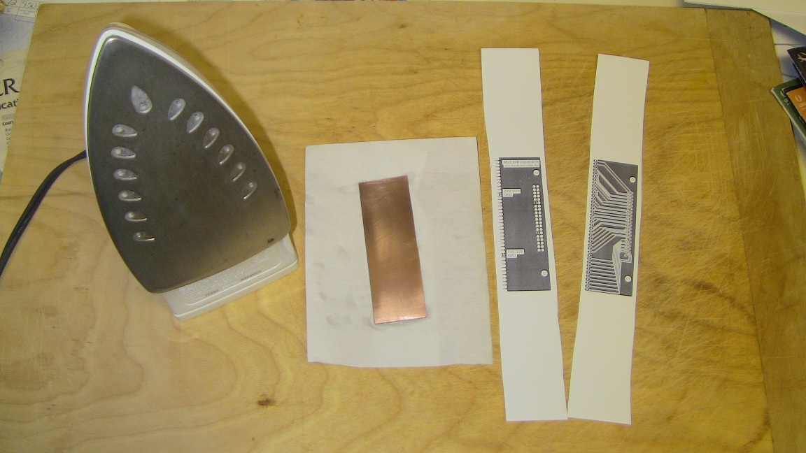
·Using an Iron, the toner is transferred to side A.

·Similarly, the toner is transferred to side B.
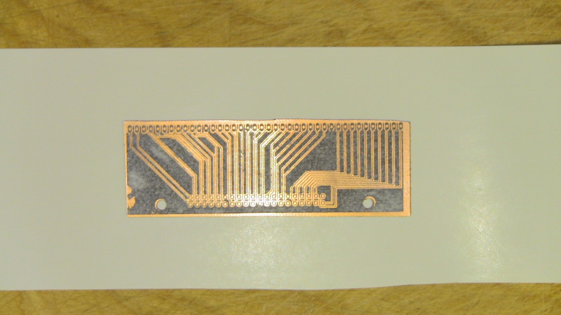
·Throw the board into a bucket of etchant and see how it comes out. You can see below, side A came out looking quite nice.
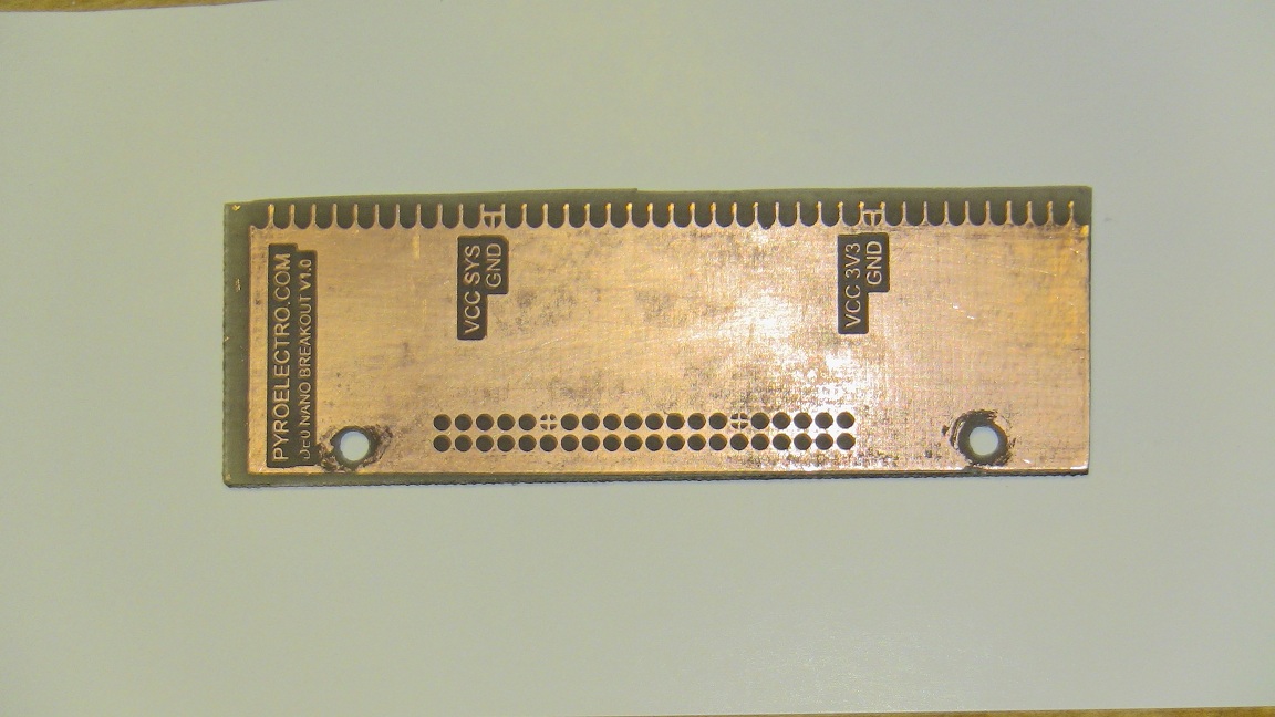
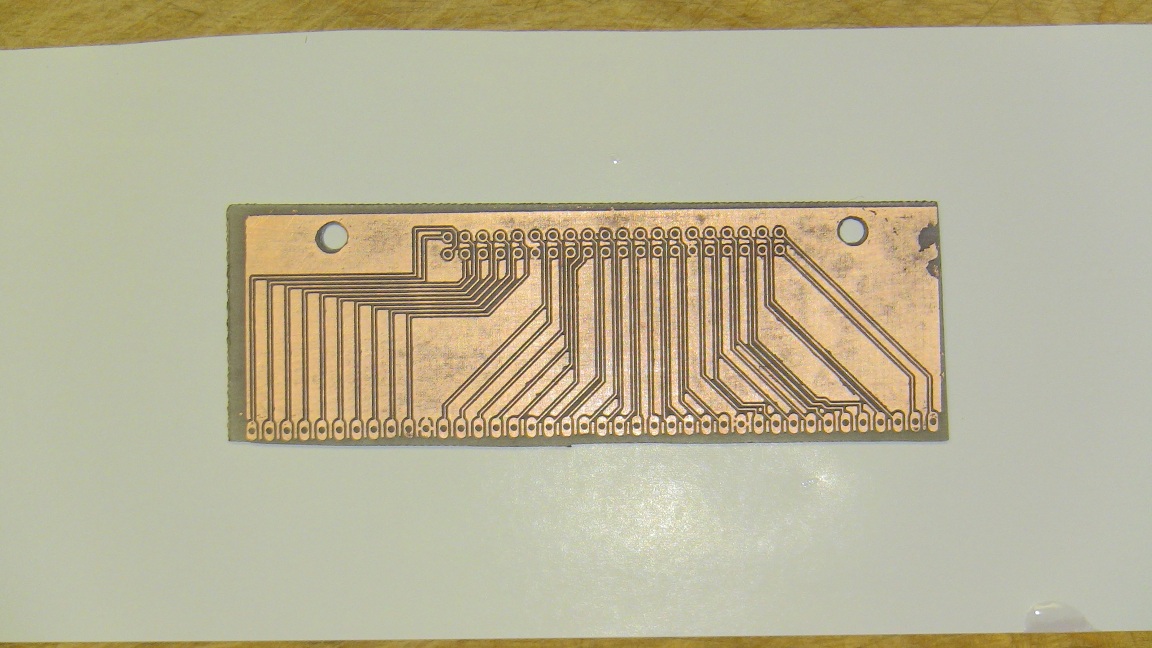
·Side B is also very clean.
·Only two parts need to be soldered into the board.
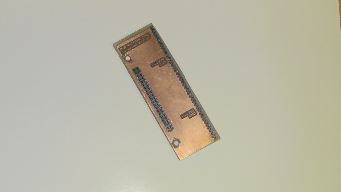
·Soldering the 80 pins down will take you a few minutes.....

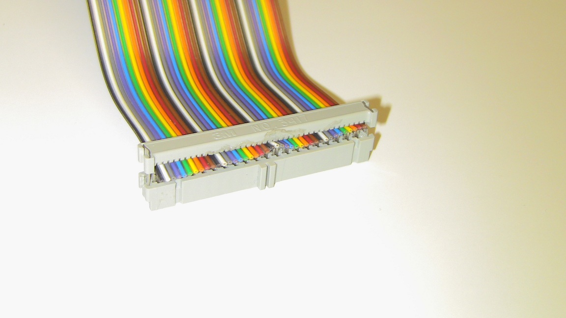
·Now let's make our own 40 pin connector cable.
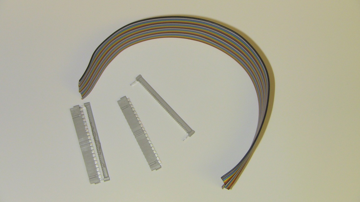
·Put the cable wire into the connector and push the connector together. Do this on both sides of the cable.
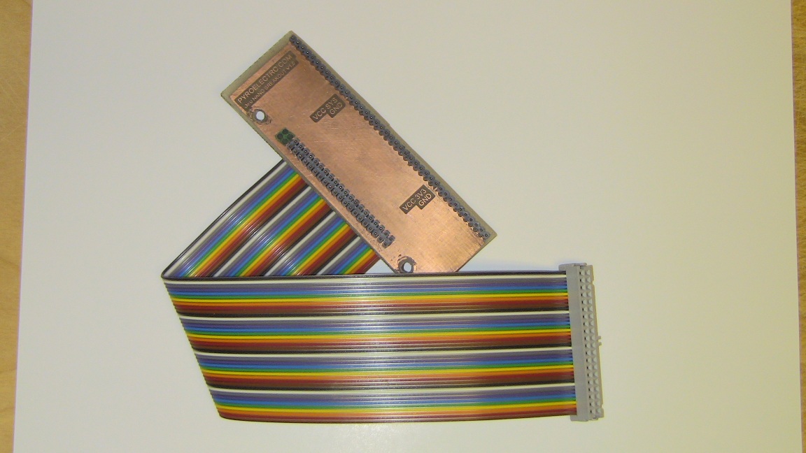
·Now our header board is complete, take a look:
·Now let's get all the LEDs connected to the breakout board.
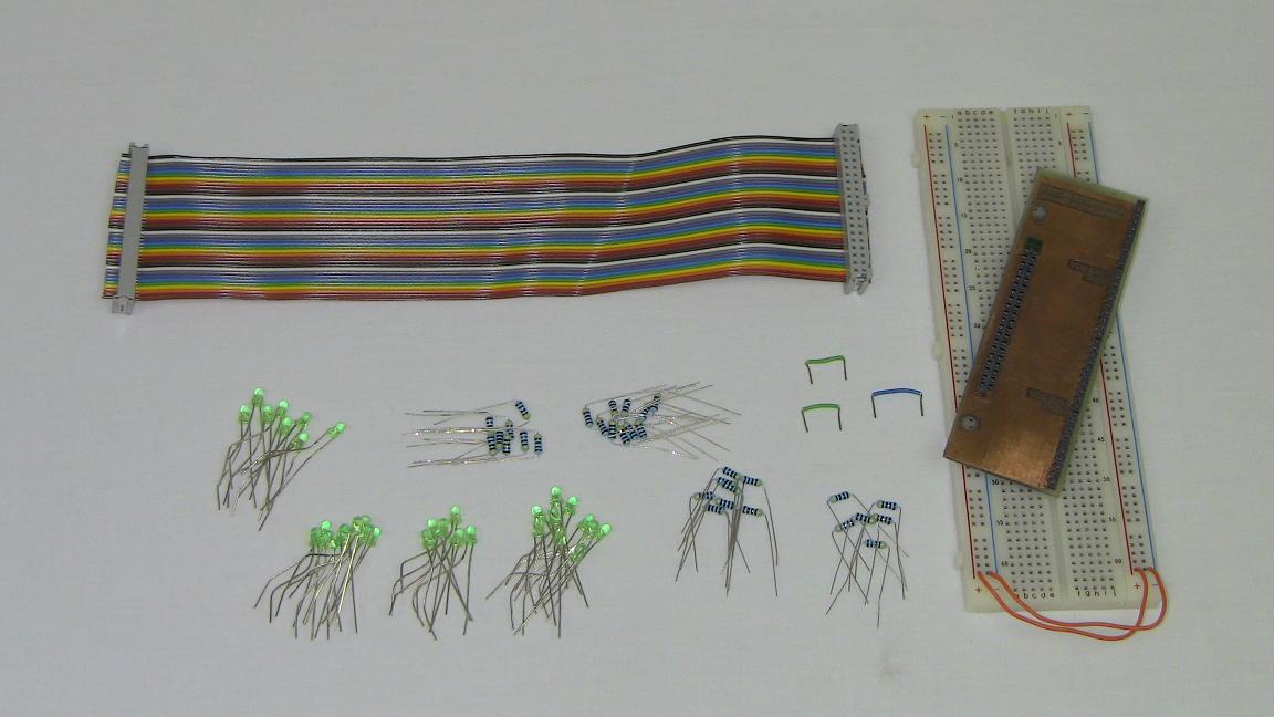
·First the ground and power connections, connect to the breadboard bus lines, then I start with the resistors and LEDs.
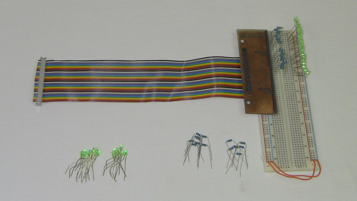
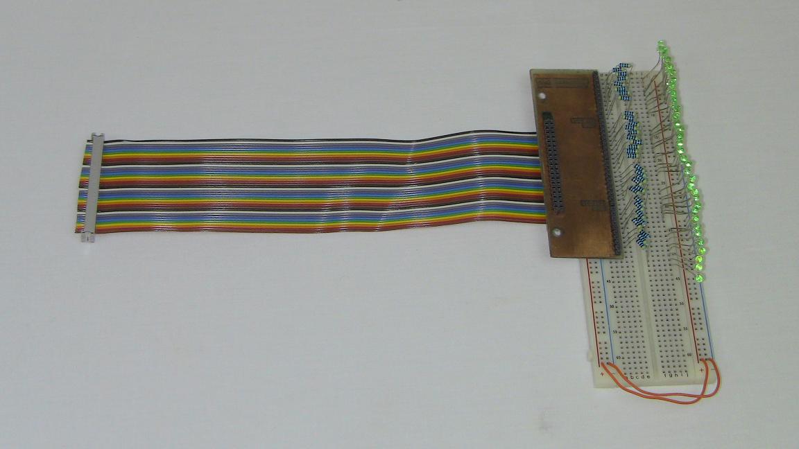
·After some time the LEDs are all wired up and ready to go. 32 of them!
·Let's see what VHDL code we'll use to test out whether or not our header expansion board works properly.