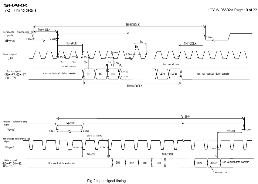
The Theory
The way the PSP LCD works is just like the way any monitor works. Pixels are output one at a time starting from the top left corner line by line until the last line is reached. Getting the timing correct is crucial or the LCD simply will not work. In total there should be 286 Horizontal Sync's per every 1 Vertical Sync. Similarly Each line of 480 pixels will take 525 clock ticks. The timing diagram pictued below elaborates on this.
PSP Display Timing Diagram

Click For Larger Image
When designing the VHDL module, the timing seen above, specifically the Vsync and Hsync signals will be followed exactly. This will lead to each pixel being displayed correctly on the screen. Understanding timing digrams can be difficult, so hope over to the forums if you have any trouble.
Frequency Timing Characteristics
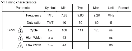
The clock signal seen in the first timing diagram above needs to adhere to the frequency timing characteristics table. Specifically the first two rows: Frequency and Duty Ratio. Ideally the clock input to the PSP LCD should be 9 MHz, but it can range from 7.83 -> 9.26 MHz. This is a great advantage for us because the wide frequency range means even if we can't hit a clock rate of 9 MHz on the date, the display will still work.
Second is the duty ratio. The clock cannot be short pulses, it needs to be +3.3v 50% of the time and 0v 50% of the time. Again, there is a range of error that is allowed. The ratio can be 40% -> 60%. So if there are short periods of clock skew or unkown delays it won't effect the system unless they are major problems.
The way the PSP LCD works is just like the way any monitor works. Pixels are output one at a time starting from the top left corner line by line until the last line is reached. Getting the timing correct is crucial or the LCD simply will not work. In total there should be 286 Horizontal Sync's per every 1 Vertical Sync. Similarly Each line of 480 pixels will take 525 clock ticks. The timing diagram pictued below elaborates on this.
Click For Larger Image
When designing the VHDL module, the timing seen above, specifically the Vsync and Hsync signals will be followed exactly. This will lead to each pixel being displayed correctly on the screen. Understanding timing digrams can be difficult, so hope over to the forums if you have any trouble.
The clock signal seen in the first timing diagram above needs to adhere to the frequency timing characteristics table. Specifically the first two rows: Frequency and Duty Ratio. Ideally the clock input to the PSP LCD should be 9 MHz, but it can range from 7.83 -> 9.26 MHz. This is a great advantage for us because the wide frequency range means even if we can't hit a clock rate of 9 MHz on the date, the display will still work.
Second is the duty ratio. The clock cannot be short pulses, it needs to be +3.3v 50% of the time and 0v 50% of the time. Again, there is a range of error that is allowed. The ratio can be 40% -> 60%. So if there are short periods of clock skew or unkown delays it won't effect the system unless they are major problems.