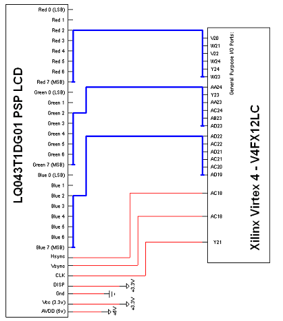
Schematic Overview
The schematic for this tutorial is for the most part straight connections from the FPGA to the PSP LCD with the exception of a few power signals coming from the power supply board.
View Full Schematic
Schematic Specifics
Missing RGB Connections
To save some time I opted to not use the lower 2 bits of each color signal. This will have very little effect on the colors output on the screen as you will see later on, and it will make our lives a little easier when wiring the hardware and coding the VHDL for the FPGA. This is an easy trick you can use to preserve 99% of the color quality and use less hardware space and pins.
Hsync, Vsync and CLK
These last few signals are what tell the LCD the what, where and how. It's important to note that the clock signal is not the FPGA clock rather a 'close to 9 MHz' signal that the LCD controller uses when refreshing the LCD display. All other connections are tied directly to power or ground.
The schematic for this tutorial is for the most part straight connections from the FPGA to the PSP LCD with the exception of a few power signals coming from the power supply board.
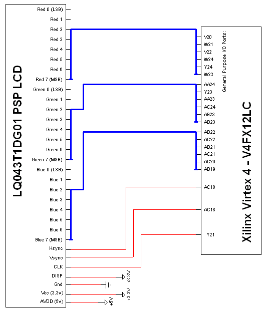
View Full Schematic
Schematic Specifics
Missing RGB Connections
To save some time I opted to not use the lower 2 bits of each color signal. This will have very little effect on the colors output on the screen as you will see later on, and it will make our lives a little easier when wiring the hardware and coding the VHDL for the FPGA. This is an easy trick you can use to preserve 99% of the color quality and use less hardware space and pins.
Hsync, Vsync and CLK
These last few signals are what tell the LCD the what, where and how. It's important to note that the clock signal is not the FPGA clock rather a 'close to 9 MHz' signal that the LCD controller uses when refreshing the LCD display. All other connections are tied directly to power or ground.