Hardware Design: PC Board Layout
Since we have built the schematic, looked into a little bit of theory for what's going on and why we're doing this, let's get to the fun stuff: Board Layout!
When it comes to board layout, there's a million different ways to lay out the same board. Some ways will naturally be better than others, just as some will be more asthetically appealing than others. Rarely do those two qualities overlap.
For this layout, I chose a more asthetically please layout with control circuitry for the LEDs on the bottom, power circuitry on the top right and the actual LEDs of a special someone's name in the middle of the board. You can see a picture of the final layout below.
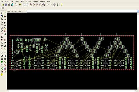
The yellow wires represent all of the net connections between the different parts. There's a lot, but not to fear, we're making a 2 layer PCB which means there should be more than enough space to route everything. So let's get routing.....I'm lazy, I admit it freely, and lazy people use the autoroute feature, while hardworking people route everything manually on their PCB. So I click the autoroute button to set everything up.
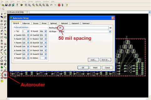
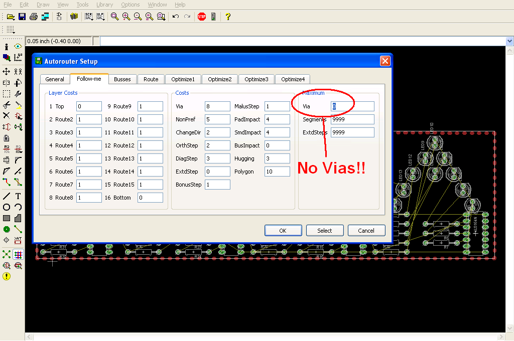
The specifics that need to be changed in this first dialog are that I want to use 50 mil spacing for the routing grid and I want to only use the Top and Bottom layers. All other routing layers should be marked "N/A" so that they aren't used. Next we need to go through The rest of the tabs and make sure no vias are used. Vias are basically a connection between the top and bottom layer. I don't want to bother with this no matter how helpful it is, at least not with this design.
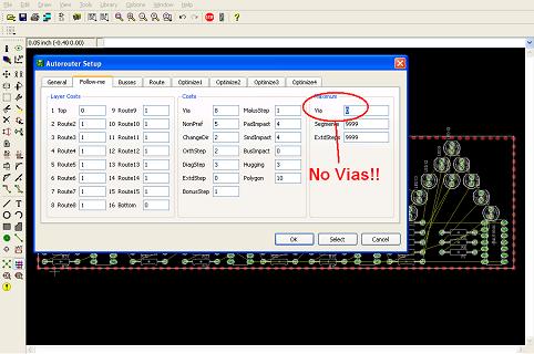
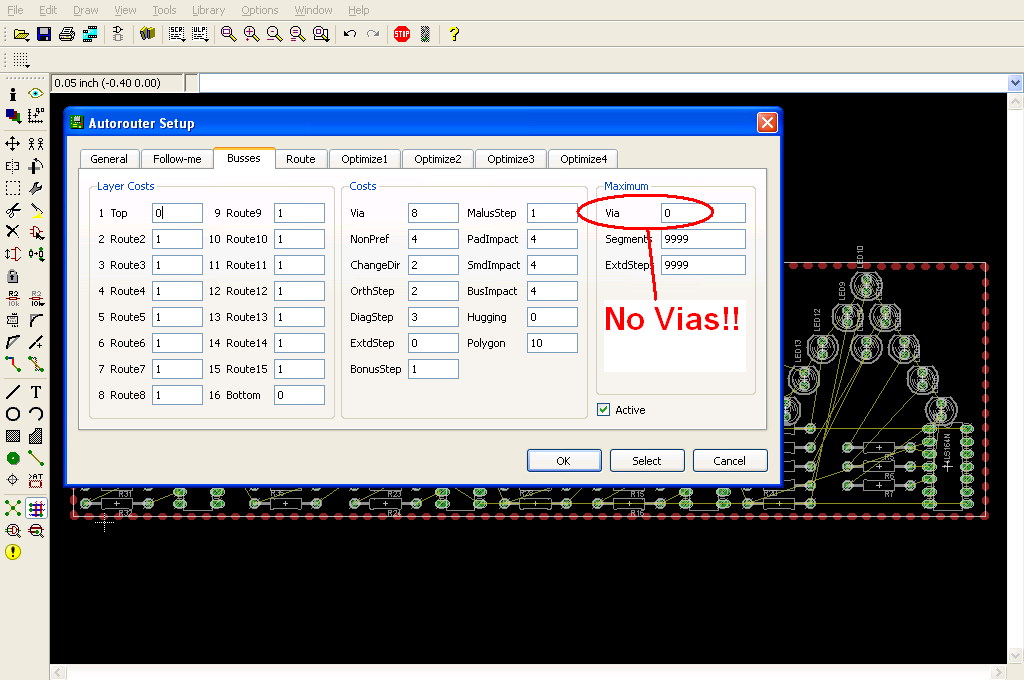
Similarly, we go through the next few tabs and put a 0 in the Vias box....this way Vias aren't used when we start the auto router.
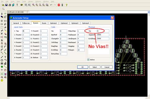
After you've selected 0 for the Vias option in all the tabs, go ahead and click ok and the autorouter will start working away. There's a lot of other customizations that the Eagle Layout Editor has, but I won't bother changing any of them. We just want to get this thing routed and ready to go.
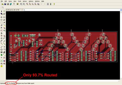
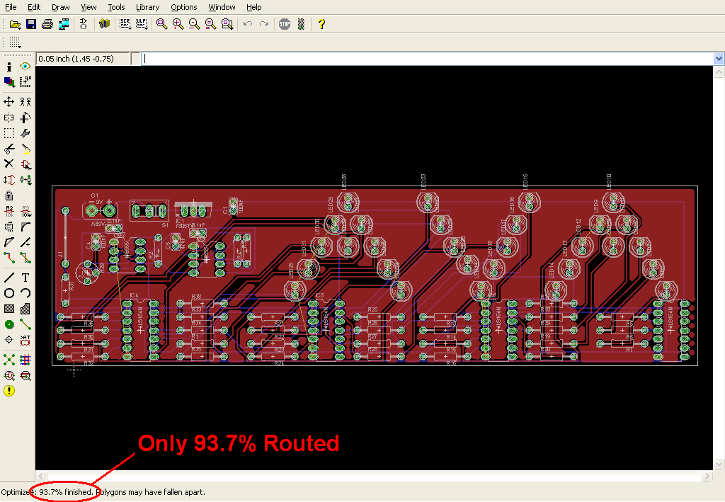
Here you can see the top/bottom layer fully routed (it can be the top or bottom Since the name 'AVA' is a palindrome it doesn't really matter). The important thing to note is that the board was only 93.7% routed. This comes to a surprise as we're using 2 layers, but often times the autorouter isn't the best in the world. So time to take a closer look at what didn't get connected.
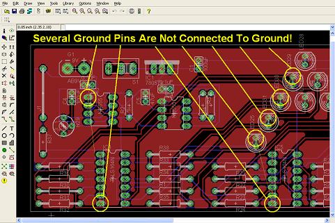
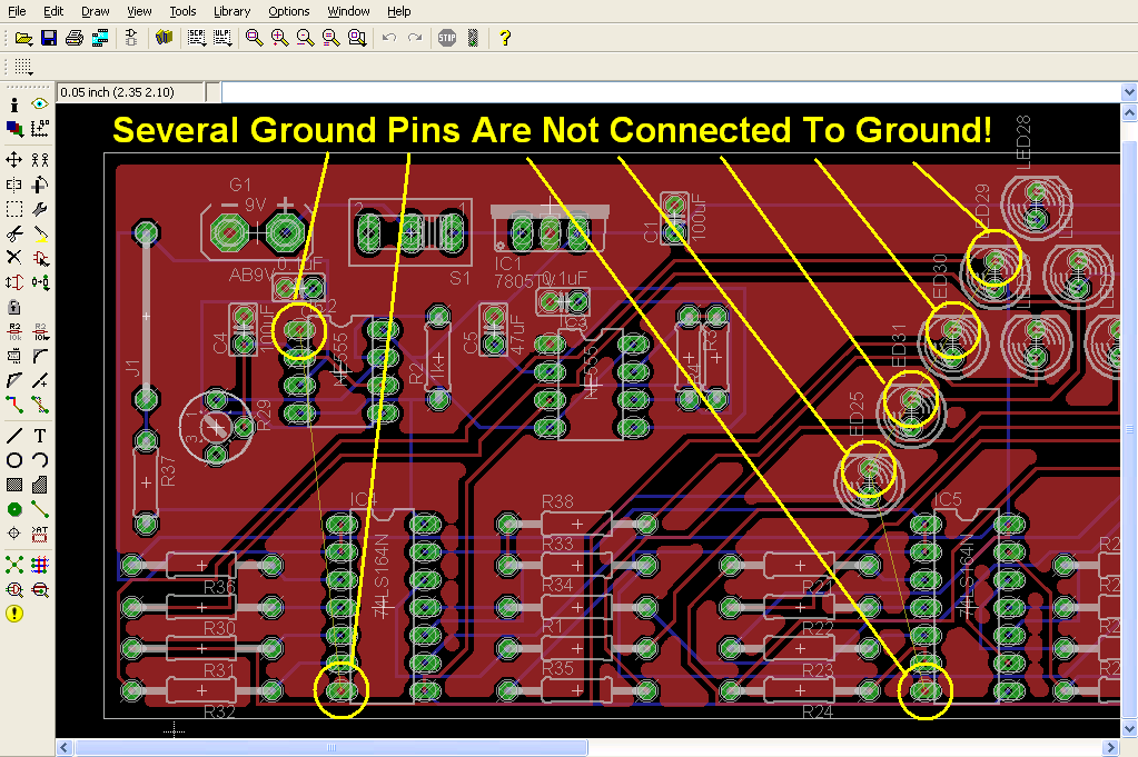
After further inspection, it becomes obvious that several pins didn't get connected to the ground plane, but everything else was routed without any problem.
Since I'm lazy, I'll call this good and just use some jumper wire to connect these last few pins to the ground plane. This isn't ideal as the point of a PCB is to not have to use wires, but I'll suffer a little extra soldering for my laziness.
Since we have built the schematic, looked into a little bit of theory for what's going on and why we're doing this, let's get to the fun stuff: Board Layout!
When it comes to board layout, there's a million different ways to lay out the same board. Some ways will naturally be better than others, just as some will be more asthetically appealing than others. Rarely do those two qualities overlap.
For this layout, I chose a more asthetically please layout with control circuitry for the LEDs on the bottom, power circuitry on the top right and the actual LEDs of a special someone's name in the middle of the board. You can see a picture of the final layout below.
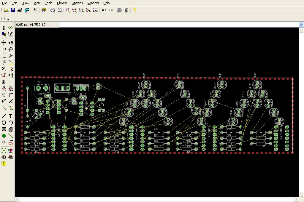
The yellow wires represent all of the net connections between the different parts. There's a lot, but not to fear, we're making a 2 layer PCB which means there should be more than enough space to route everything. So let's get routing.....I'm lazy, I admit it freely, and lazy people use the autoroute feature, while hardworking people route everything manually on their PCB. So I click the autoroute button to set everything up.
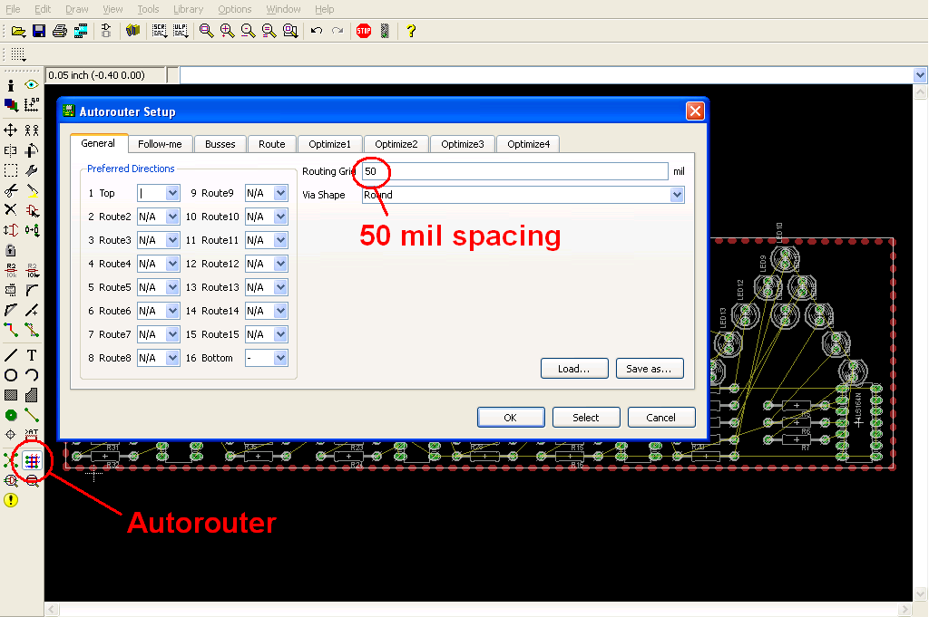
The specifics that need to be changed in this first dialog are that I want to use 50 mil spacing for the routing grid and I want to only use the Top and Bottom layers. All other routing layers should be marked "N/A" so that they aren't used. Next we need to go through The rest of the tabs and make sure no vias are used. Vias are basically a connection between the top and bottom layer. I don't want to bother with this no matter how helpful it is, at least not with this design.
Similarly, we go through the next few tabs and put a 0 in the Vias box....this way Vias aren't used when we start the auto router.
After you've selected 0 for the Vias option in all the tabs, go ahead and click ok and the autorouter will start working away. There's a lot of other customizations that the Eagle Layout Editor has, but I won't bother changing any of them. We just want to get this thing routed and ready to go.
Here you can see the top/bottom layer fully routed (it can be the top or bottom Since the name 'AVA' is a palindrome it doesn't really matter). The important thing to note is that the board was only 93.7% routed. This comes to a surprise as we're using 2 layers, but often times the autorouter isn't the best in the world. So time to take a closer look at what didn't get connected.
After further inspection, it becomes obvious that several pins didn't get connected to the ground plane, but everything else was routed without any problem.
Since I'm lazy, I'll call this good and just use some jumper wire to connect these last few pins to the ground plane. This isn't ideal as the point of a PCB is to not have to use wires, but I'll suffer a little extra soldering for my laziness.