Theory: Why Do We Need 2 Layers?
First I will discuss why a two layer board will be necessary for this project, then I'll explain how the circuit 'theoretically' works. This project is going to have a lot of data lines. Since many LEDs are going to be used and each LED is going to demand a resistor, even with a ground plan, that's several unique lines going across the board. True, with a perfect board layout it might be possible to put this design on one plane, but we're in a hurry to get this design done and more importantly I want to make it 2 layers anyway which means its ok to be a little lazy at this point.
An important thing to note when you are building a schematic is what the pin out of the actual chip looks like. This lone fact, more often than not, will tell you if a single layer board will even be possible. Many 74xx series chips integrate nicely into single layer boards as they were designed with simplicity in mind, however not all of them do as we'll later on when we lay the board out and route it.
Theory: What Does The Circuit Do?
The GIF image above illustrates better than any words could what the circuit should do when finished and running. The 555 timers are busy sending digital +5v and +0v signals out to the 74LS164's clocking in input. Depending on the trimpot's value there will be many sequential LEDs lit up, or there will be very few.
Theory: A Close Look At The 555 Signals
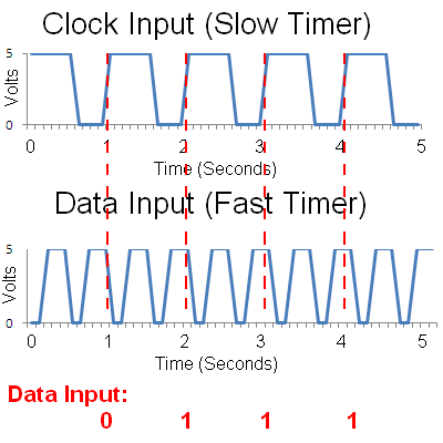
The actual signals output by the 555 Timers are seen in the above illustrations. You can see how the trimpot resistor value allows for either overlap of the true clock signal or for a much quicker signal than that of the clock. Each different case will have a different effect on the data output to the LEDs, make either more or fewer LEDs lit up at once.
First I will discuss why a two layer board will be necessary for this project, then I'll explain how the circuit 'theoretically' works. This project is going to have a lot of data lines. Since many LEDs are going to be used and each LED is going to demand a resistor, even with a ground plan, that's several unique lines going across the board. True, with a perfect board layout it might be possible to put this design on one plane, but we're in a hurry to get this design done and more importantly I want to make it 2 layers anyway which means its ok to be a little lazy at this point.
An important thing to note when you are building a schematic is what the pin out of the actual chip looks like. This lone fact, more often than not, will tell you if a single layer board will even be possible. Many 74xx series chips integrate nicely into single layer boards as they were designed with simplicity in mind, however not all of them do as we'll later on when we lay the board out and route it.
The GIF image above illustrates better than any words could what the circuit should do when finished and running. The 555 timers are busy sending digital +5v and +0v signals out to the 74LS164's clocking in input. Depending on the trimpot's value there will be many sequential LEDs lit up, or there will be very few.
The actual signals output by the 555 Timers are seen in the above illustrations. You can see how the trimpot resistor value allows for either overlap of the true clock signal or for a much quicker signal than that of the clock. Each different case will have a different effect on the data output to the LEDs, make either more or fewer LEDs lit up at once.