Schematic Overview
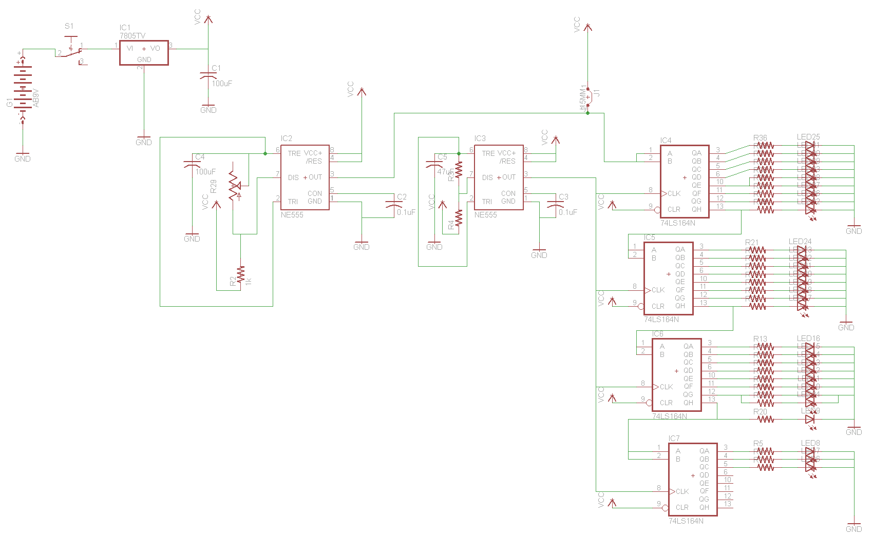
For the 2 layer board schematic, we'll use 6 core IC's: 4 74LS164's and 2 555 Timers. The schematic will be built using Eagle Layout Editor since all the parts I need exist in their library. The final schematic can be seen below, click on the picture for the full view.
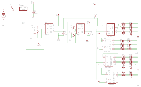
View Full Schematic
Schematic Specifics
Dual 555 Timers
Two 555 timers are used in this circuit. The first 555 timer uses two 10kΩ resistors and a 47uF capacitor, which creates an output signal that alternates between +0v and +5v every second. This clock signal will therefore shift in data to the 74LS164's 1 bit every 1 second. The second 555 timer output signal will be fed into the data input of the 74LS164. It uses one 1kΩ resistor, a 100uF capacitor and a 100kΩ trimpot (variable resistor). When the trimpot is varied from 100kΩ to 0Ω, the 555 timer output frequency changes from 14 Hz to 0.1 Hz.
74LS164 - Serial Data Input, Parallel Data Output
These shift registers will receive data input from the slower clock, which is input whenever the faster clock transitions from +0v to +5v. This means the data input will be constant since the two clocks work off of one another. Only when the trimpot is changed will the data input change, as this makes the faster clock speed up or slow down. If the slow clock ever becomes faster than the fast clock, the digital data input will always be seen as 1.
For the 2 layer board schematic, we'll use 6 core IC's: 4 74LS164's and 2 555 Timers. The schematic will be built using Eagle Layout Editor since all the parts I need exist in their library. The final schematic can be seen below, click on the picture for the full view.
View Full Schematic
Schematic Specifics
Dual 555 Timers
Two 555 timers are used in this circuit. The first 555 timer uses two 10kΩ resistors and a 47uF capacitor, which creates an output signal that alternates between +0v and +5v every second. This clock signal will therefore shift in data to the 74LS164's 1 bit every 1 second. The second 555 timer output signal will be fed into the data input of the 74LS164. It uses one 1kΩ resistor, a 100uF capacitor and a 100kΩ trimpot (variable resistor). When the trimpot is varied from 100kΩ to 0Ω, the 555 timer output frequency changes from 14 Hz to 0.1 Hz.
74LS164 - Serial Data Input, Parallel Data Output
These shift registers will receive data input from the slower clock, which is input whenever the faster clock transitions from +0v to +5v. This means the data input will be constant since the two clocks work off of one another. Only when the trimpot is changed will the data input change, as this makes the faster clock speed up or slow down. If the slow clock ever becomes faster than the fast clock, the digital data input will always be seen as 1.