Schematic Overview
To be completely honest, I'm not even sure if a schematic is necessary because this is a drop dead simple design in terms of hardware. Below is a high-level block design of how everything is wired up. If it looks too simple to be true, well it's just really simple!
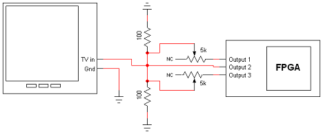
View Full Schematic
Schematic Specifics
Signal Voltage Divider
Three signals will be coming out of the FPGA. Output 1 is used for the display portion of the signal (voltage divider to 0.5v), Output 2 will be a 3.3v signal with represents maximum color intesity for the display and Output 3 signal will take care of the horizontal and vertical sync signals (voltage divider to 0.3v). After they go through the voltage divider they are mixed together and send to the TV. You will have to test the two voltage dividers with a steady 3.3v input to make sure they are set or the correct peak voltage.
FPGA Timing
The FPGA being used will run at a frequency of 100 MHz which means 10 nanoseconds per clock cycle. This gives us ultimate control to build a perfect NTSC video signal to input into the TV. The standard itsself measures everything in 0.1uS which is 10 nanoseconds, this means we have more than enough time to get all decisions made and can output properly with no rush.
To be completely honest, I'm not even sure if a schematic is necessary because this is a drop dead simple design in terms of hardware. Below is a high-level block design of how everything is wired up. If it looks too simple to be true, well it's just really simple!
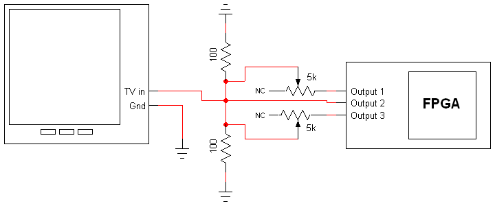
View Full Schematic
Schematic Specifics
Signal Voltage Divider
Three signals will be coming out of the FPGA. Output 1 is used for the display portion of the signal (voltage divider to 0.5v), Output 2 will be a 3.3v signal with represents maximum color intesity for the display and Output 3 signal will take care of the horizontal and vertical sync signals (voltage divider to 0.3v). After they go through the voltage divider they are mixed together and send to the TV. You will have to test the two voltage dividers with a steady 3.3v input to make sure they are set or the correct peak voltage.
FPGA Timing
The FPGA being used will run at a frequency of 100 MHz which means 10 nanoseconds per clock cycle. This gives us ultimate control to build a perfect NTSC video signal to input into the TV. The standard itsself measures everything in 0.1uS which is 10 nanoseconds, this means we have more than enough time to get all decisions made and can output properly with no rush.