Schematic Overview
The FPGA VGA Resistor DAC circuit is not terribly difficult however it will take some double checking to make sure you have everything hooked up properly before working the first time. The main devices used in the circuit are the EPM7128, VGA Connector and 7805 +5v Reg.
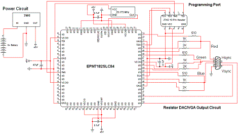
View Full Schematic
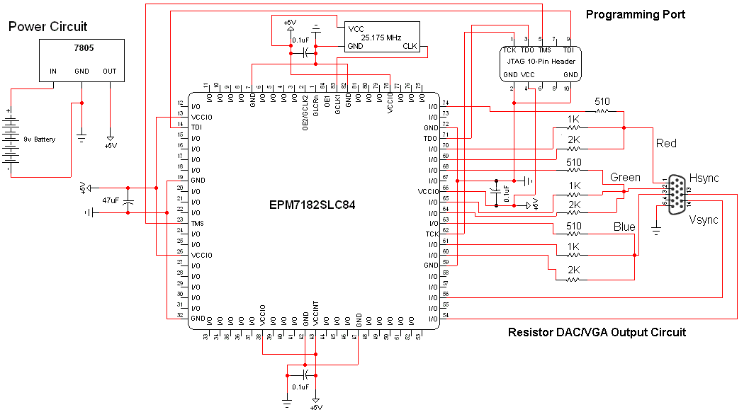
Schematic Specifics
Power Circuit
This is a basic power circuit, the battery connects to the input terminal of the 7805, which regulates down to +5v for the output. Be sure to use some capacitors on all the Vdd/Vss inputs around the CPLD. This will allow the CPLD to function properly.
VGA Output Circuit
The VGA circuit consists of 9 resistors, the VGA connector and a bunch of wire wrap. Each resistor is connected to a specific I/O pin on the CPLD and then each group of 510/1k/2k are tied together with one of the Red, Green or Blue VGA color signals. This is how we get the proper output analog voltages for VGA.
Programming Circuit
The programming circuit consists of properly connecting wires to the 10 pin shrouded header. Double and triple check that you connect these up correctly or you might harm the programmer or the CPLD.
The FPGA VGA Resistor DAC circuit is not terribly difficult however it will take some double checking to make sure you have everything hooked up properly before working the first time. The main devices used in the circuit are the EPM7128, VGA Connector and 7805 +5v Reg.
View Full Schematic
Schematic Specifics
Power Circuit
This is a basic power circuit, the battery connects to the input terminal of the 7805, which regulates down to +5v for the output. Be sure to use some capacitors on all the Vdd/Vss inputs around the CPLD. This will allow the CPLD to function properly.
VGA Output Circuit
The VGA circuit consists of 9 resistors, the VGA connector and a bunch of wire wrap. Each resistor is connected to a specific I/O pin on the CPLD and then each group of 510/1k/2k are tied together with one of the Red, Green or Blue VGA color signals. This is how we get the proper output analog voltages for VGA.
Programming Circuit
The programming circuit consists of properly connecting wires to the 10 pin shrouded header. Double and triple check that you connect these up correctly or you might harm the programmer or the CPLD.