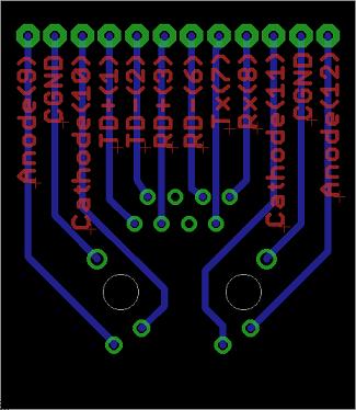
Make The PCB Design
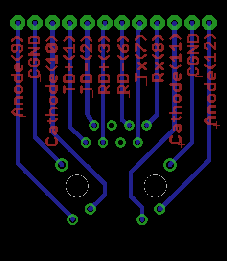
Now that we have a schematic built, the board is laid out with SIPs set to 0.1". The picture below shows what the final board layout looks like in the eagle layout editor.
PCB Fabrication Process
Now we will go through the process of transferring the toner from the glossy laser printer paper to the PCB and then etching/drilling the PCB.

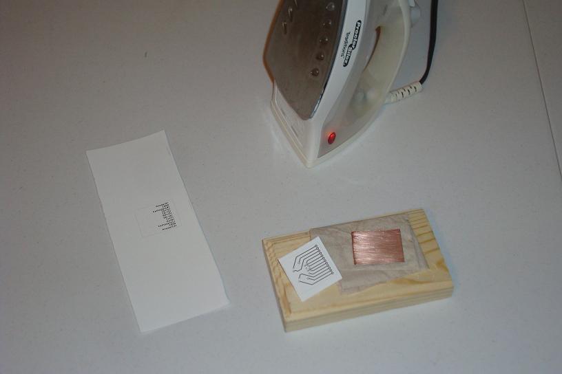
·First print out the board layout from your laser printer on glossy paper and cut the paper to the size of the board.
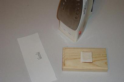
·Align your design face down on the PCB, then apply heat with the iron all over the board. (5-10 min)
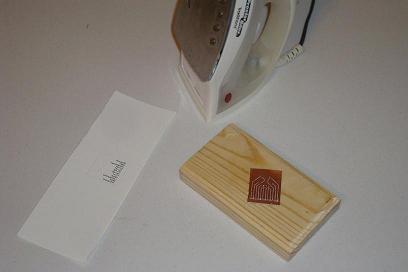
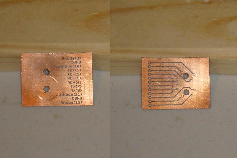
·Soak the board in water and pull off the glossy paper. Repeat For 2nd Layer.

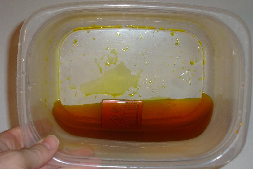
·Place the board in a mixture of Ferric Chloride + Hot Water.

·10-20 minutes later the board is etched.
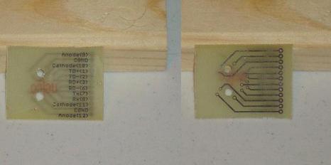
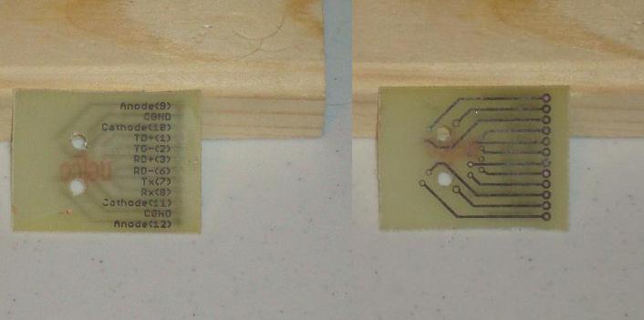
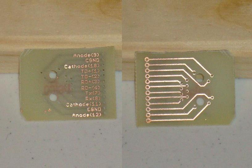
·Scrub off the remaining toner to see the copper traces.
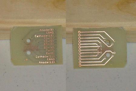
·The PCB is made, and ready to be populated with parts.
Now that we have a schematic built, the board is laid out with SIPs set to 0.1". The picture below shows what the final board layout looks like in the eagle layout editor.
PCB Fabrication Process
Now we will go through the process of transferring the toner from the glossy laser printer paper to the PCB and then etching/drilling the PCB.
·First print out the board layout from your laser printer on glossy paper and cut the paper to the size of the board.

·Align your design face down on the PCB, then apply heat with the iron all over the board. (5-10 min)

·Soak the board in water and pull off the glossy paper. Repeat For 2nd Layer.
·Place the board in a mixture of Ferric Chloride + Hot Water.
·10-20 minutes later the board is etched.
·Scrub off the remaining toner to see the copper traces.
·The PCB is made, and ready to be populated with parts.