Schematic Overview
The schematic seen below is actually pulled straight from the datasheet of the ByteBlasterMV (hopefully altera doesn't mind me copying it for you guys). After the schematic I gave brief explanations of the most important parts. The main parts in the schematic are the 74_244, Parallel Port Connector and 10 Pin Connector.
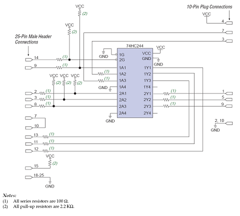
View Full Schematic
Schematic Specifics
25 Pin Male Header
Not all of the parallel port's 25 pins are actually connected to something, however the bulk of them, pins: #18-25 are connected to ground. The left side of the schematic represents all connections to be made to the parallel port connector. Connecting pin 7 to 10 on the connector acts as the ID circuitry, telling Quartus II that this is a ByteBlasterMV programmer.
10 Pin Female Connector
Similarly, not all the pins on this connector are used. However the ones that are can be seen on the right side of the schematic. These will connect up to the CPLD/FPGA when it comes time to program it.
Resistors
Two types of resistors are used in the schematic seen above listed as (1) or (2). The bulk of the resistors are 100Ω resistors off of the input or outputs. The remaining resistors are 2.2kΩ pull-up to +5v resistors. I will substitute 1kΩ resistors instead because I had them laying around. If you have 2.2kΩ follow the schematic!
The schematic seen below is actually pulled straight from the datasheet of the ByteBlasterMV (hopefully altera doesn't mind me copying it for you guys). After the schematic I gave brief explanations of the most important parts. The main parts in the schematic are the 74_244, Parallel Port Connector and 10 Pin Connector.
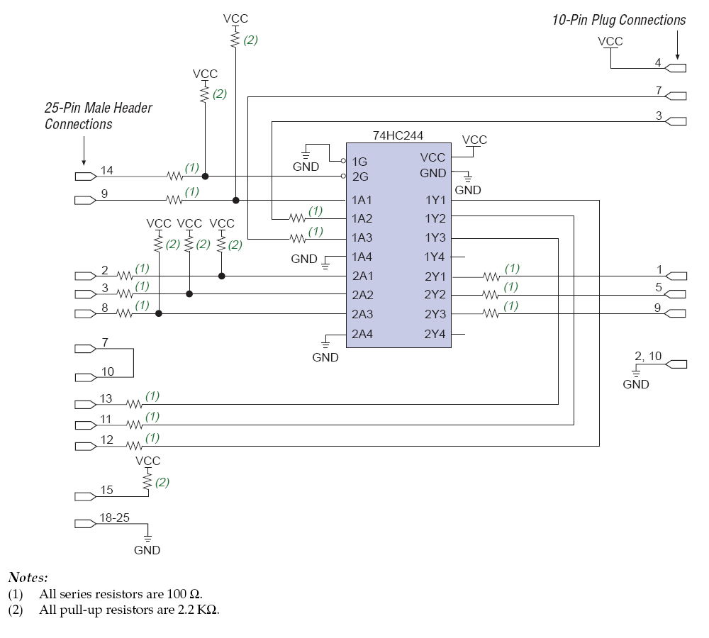
View Full Schematic
Schematic Specifics
25 Pin Male Header
Not all of the parallel port's 25 pins are actually connected to something, however the bulk of them, pins: #18-25 are connected to ground. The left side of the schematic represents all connections to be made to the parallel port connector. Connecting pin 7 to 10 on the connector acts as the ID circuitry, telling Quartus II that this is a ByteBlasterMV programmer.
10 Pin Female Connector
Similarly, not all the pins on this connector are used. However the ones that are can be seen on the right side of the schematic. These will connect up to the CPLD/FPGA when it comes time to program it.
Resistors
Two types of resistors are used in the schematic seen above listed as (1) or (2). The bulk of the resistors are 100Ω resistors off of the input or outputs. The remaining resistors are 2.2kΩ pull-up to +5v resistors. I will substitute 1kΩ resistors instead because I had them laying around. If you have 2.2kΩ follow the schematic!