The schematic showed you how the actual design is not very complex and relies on only a handful of parts. The design was meant to be this way, because after all we also have to make th PCB, so why not keep things simple.
Making The AV Test PCB
The process shown below is somewhat abridged and assumes you're familiar and confident with making your own PCB's at home. The DIY 2 Layer PCB tutorial can serve as a better guide on how to get your own PCB's working.
·Print the design on glossy paper and print it out for transferring.
·Top side has been toner-transffered. Two holes were drilled to line up the bottom side for toner transfer.
·Toner transferred to the board for the bottom side of the PCB, etching time!
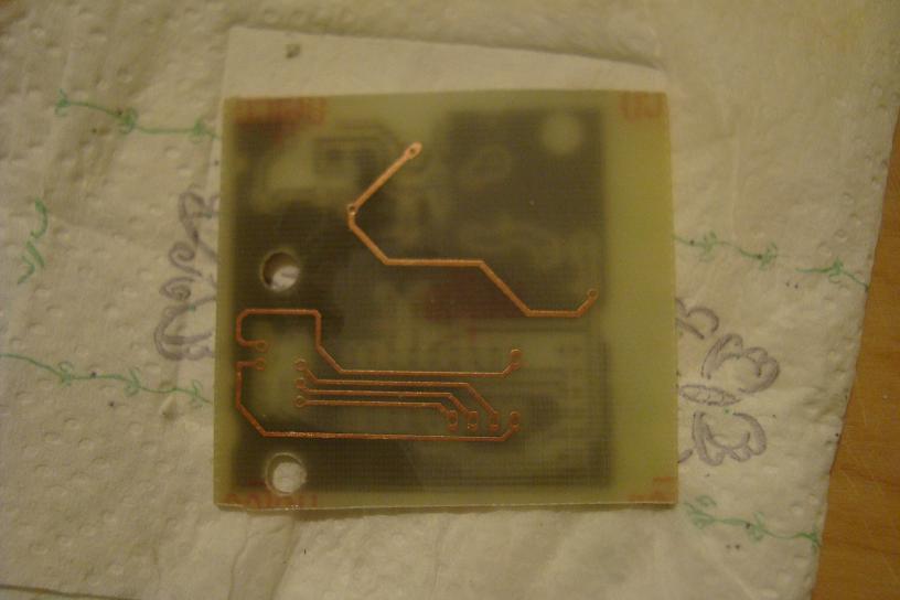
·Only the copper we want is left behind from the etching process.

·Holding the board up to the light we can see that both sides of the PCB match up virtually perfectly. This is a difficult feat to accomplish and might take a few tries to get just right.