Project Info
Author: Chris
Difficulty: Medium
Time Invested: 7 Hours
Prerequisites:
Take a look at the above
tutorials before continuing
to read this tutorial.
Author: Chris
Difficulty: Medium
Time Invested: 7 Hours
Prerequisites:
- Homemade PCB (Etching)
- Wear Gloves Around The Etching Solution
Take a look at the above
tutorials before continuing
to read this tutorial.
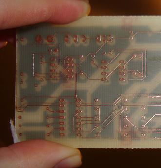
In PCB Design for hobbyists, 1 layer PCB's are usually enough to do the trick. However, when you evolve and start building more complex circuits you will need a second layer (or even more!) so that all the electronics in your project can be connected together.
Purpose & Overview of this project
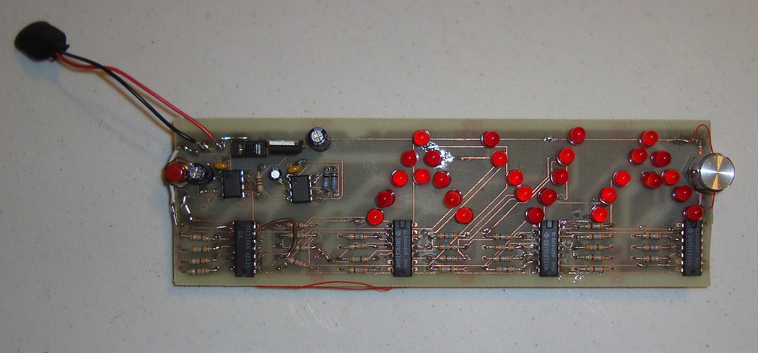
This tutorial proposes to successully design (using Eagle Layout Editor), etch and build a 2 layer PCB board. The example design will be a simple 'led' flasher circuit that I'll give to someone special for their birthday! The circuit will have two 555 timers clocking in data to some 74ls164 (serial in - parallel out) registers. With a variable resistor trimpot to speed up or slow down the LED transitions.
Understanding how the design itsself will work is not as important as is understanding the process for building the design in Eagle Layout (or the layout program of your choice) and going through the toner transfer and etching process. So pay more attention to the step-by-step process and not so much attention to the details of the circuit design.