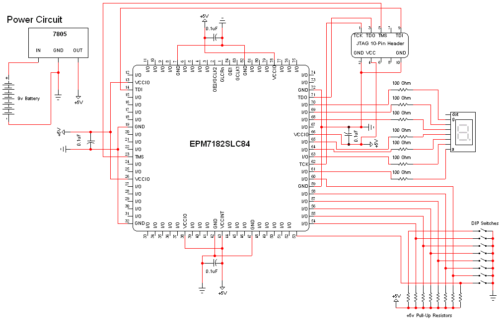
Schematic Overview
The schematic is very similar to the one seen in the CPLD Development Board Tutorial because it's basically the same board with a tiny addition. The new part of the schematic is in the lower right corner. 8 (DIP) Switches, a resistor array & some additional wiring. Notice the pins that the switches are connected to on the CPLD, these will be important later on when you choose I/O pins in the program.

View Full Schematic
Schematic Specifics
Power Circuit
The power circuit is a 9v Battery hooked up to the LM7805 with several capacitors attached to output & ground of the LM7805 to keep a steady 5v DC.
Programming Circuit
The programming circuit uses a "shrouded header" with 10 pins. This is a standard JTAG header. We will use this to program the CPLD with the ByteBlaster MV cable. Double check the wiring on this part of the board otherwise you might fry your ByteBlaster cable!
7 Segment LED Display
The 7 segment led display is wired up to 7 pins between 61-70 on the CPLD. These 7 pins control which leds are lit up inside the display. For our purposes in this project we'll only make a simple program that lights them all up, nothing too fancy. The 100 resistors that precede the display are just current limiting resistors.
8 DIP Switches & Resistor Array
These allow the user to give input and ultimately decide what is to be displayed on the 7-Segment LED Display. Depending upon which bit is set, the corresponding number will be displayed on the display (1->1, 2->2, etc.).
The schematic is very similar to the one seen in the CPLD Development Board Tutorial because it's basically the same board with a tiny addition. The new part of the schematic is in the lower right corner. 8 (DIP) Switches, a resistor array & some additional wiring. Notice the pins that the switches are connected to on the CPLD, these will be important later on when you choose I/O pins in the program.
View Full Schematic
Schematic Specifics
Power Circuit
The power circuit is a 9v Battery hooked up to the LM7805 with several capacitors attached to output & ground of the LM7805 to keep a steady 5v DC.
Programming Circuit
The programming circuit uses a "shrouded header" with 10 pins. This is a standard JTAG header. We will use this to program the CPLD with the ByteBlaster MV cable. Double check the wiring on this part of the board otherwise you might fry your ByteBlaster cable!
7 Segment LED Display
The 7 segment led display is wired up to 7 pins between 61-70 on the CPLD. These 7 pins control which leds are lit up inside the display. For our purposes in this project we'll only make a simple program that lights them all up, nothing too fancy. The 100 resistors that precede the display are just current limiting resistors.
8 DIP Switches & Resistor Array
These allow the user to give input and ultimately decide what is to be displayed on the 7-Segment LED Display. Depending upon which bit is set, the corresponding number will be displayed on the display (1->1, 2->2, etc.).