The Theory
SPI has no formal definition, just a lose set of guidelines that manufacturers follow so this means any SPI master interface must be flexible. This theory section will be split into two parts, the first part where we will look at a standard SPI Write and SPI Read and the second part, where we will look at a custom single byte SPI Write.
The 4 Clock Modes Of SPI
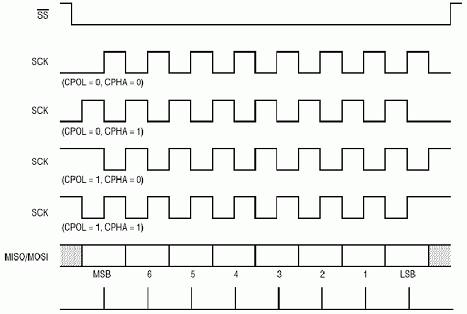
Before we dive deep into the SPI Write and SPI Read timing diagrams, it's important to note that 4 types of SPI clocking exist. What this means is that the SPI slave device won't actually accept the current bit of data unless the certain clock state (rising edge or falling edge) is detected. Two additional parameters exist and that is whether the clock is a +5v or +0v when the SPI interface is idle. These 4 scenarios give you the timing diagram seen above.
A Standard SPI Write

To write to a register on an SPI slave device, typically you send the address (MSB - most significant bit first) and then the data (MSB). The first bit of an SPI write command is the Read/Write* bit, telling the SPI slave whether you intend to read or write to/from it. There are some variations of SPI write commands, so always check the datasheet of the slave device you intend to use.
A Standard SPI Read

To read registers on an SPI slave device, typically you send the first Read/Write bit (set to read) and then a 7 bit address. The slave device will return the contents of the register on the MISO connection. In the case above, the registers are 8 bit, so 8 bits of data is returned to the master.
SPI has no formal definition, just a lose set of guidelines that manufacturers follow so this means any SPI master interface must be flexible. This theory section will be split into two parts, the first part where we will look at a standard SPI Write and SPI Read and the second part, where we will look at a custom single byte SPI Write.

Before we dive deep into the SPI Write and SPI Read timing diagrams, it's important to note that 4 types of SPI clocking exist. What this means is that the SPI slave device won't actually accept the current bit of data unless the certain clock state (rising edge or falling edge) is detected. Two additional parameters exist and that is whether the clock is a +5v or +0v when the SPI interface is idle. These 4 scenarios give you the timing diagram seen above.
To write to a register on an SPI slave device, typically you send the address (MSB - most significant bit first) and then the data (MSB). The first bit of an SPI write command is the Read/Write* bit, telling the SPI slave whether you intend to read or write to/from it. There are some variations of SPI write commands, so always check the datasheet of the slave device you intend to use.
To read registers on an SPI slave device, typically you send the first Read/Write bit (set to read) and then a 7 bit address. The slave device will return the contents of the register on the MISO connection. In the case above, the registers are 8 bit, so 8 bits of data is returned to the master.