Breakout Board:
Eagle Project Files
VGA_Breakout.sch
VGA_Breakout.brd
Board Artwork VGA_Breakout.pdf
Eagle Project Files
VGA_Breakout.sch
VGA_Breakout.brd
Board Artwork VGA_Breakout.pdf
There are two main pieces of hardware that go with this project. The first is the DE0 Nano Development board (seen below). This is the board will all the intelligence and the FPGA that we will be programming. Since this board doesn't have any display port, we'll need to build one. So, the second piece of hardware is a smalle VGA breakout board.
DE0 Nano Development Board
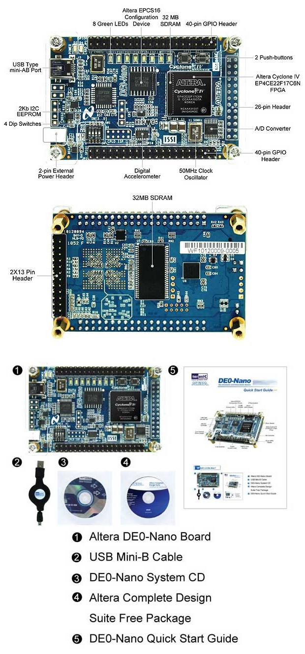
This 'tiny' development board packs a large punch because of all the extra features it has. RAM, ROM, Accelerometer, Tons of I/O, LEDs, Push Buttons and a gigantic FPGA to go with it all.
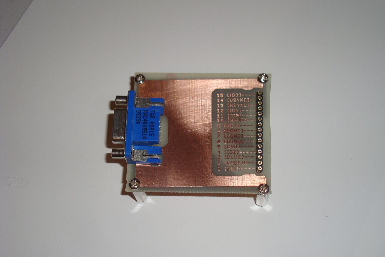
Building The VGA Breakout Board
We will use the toner-transfer process to get the PCB artwork onto both sides of the board. A quick advisory: if you're using ferric chloride as an etchant, wear gloves, goggles and safety gear. That stuff isn't very friendly to biological life.
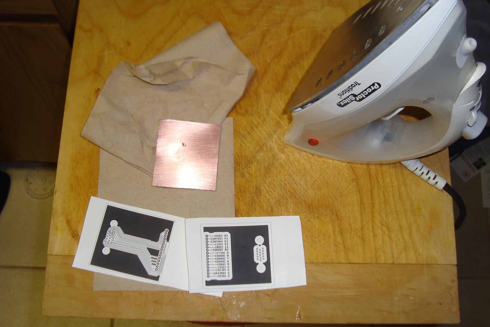
·Using an Iron, the toner is transferred to side A.
·Similarly, the toner is transferred to side B.
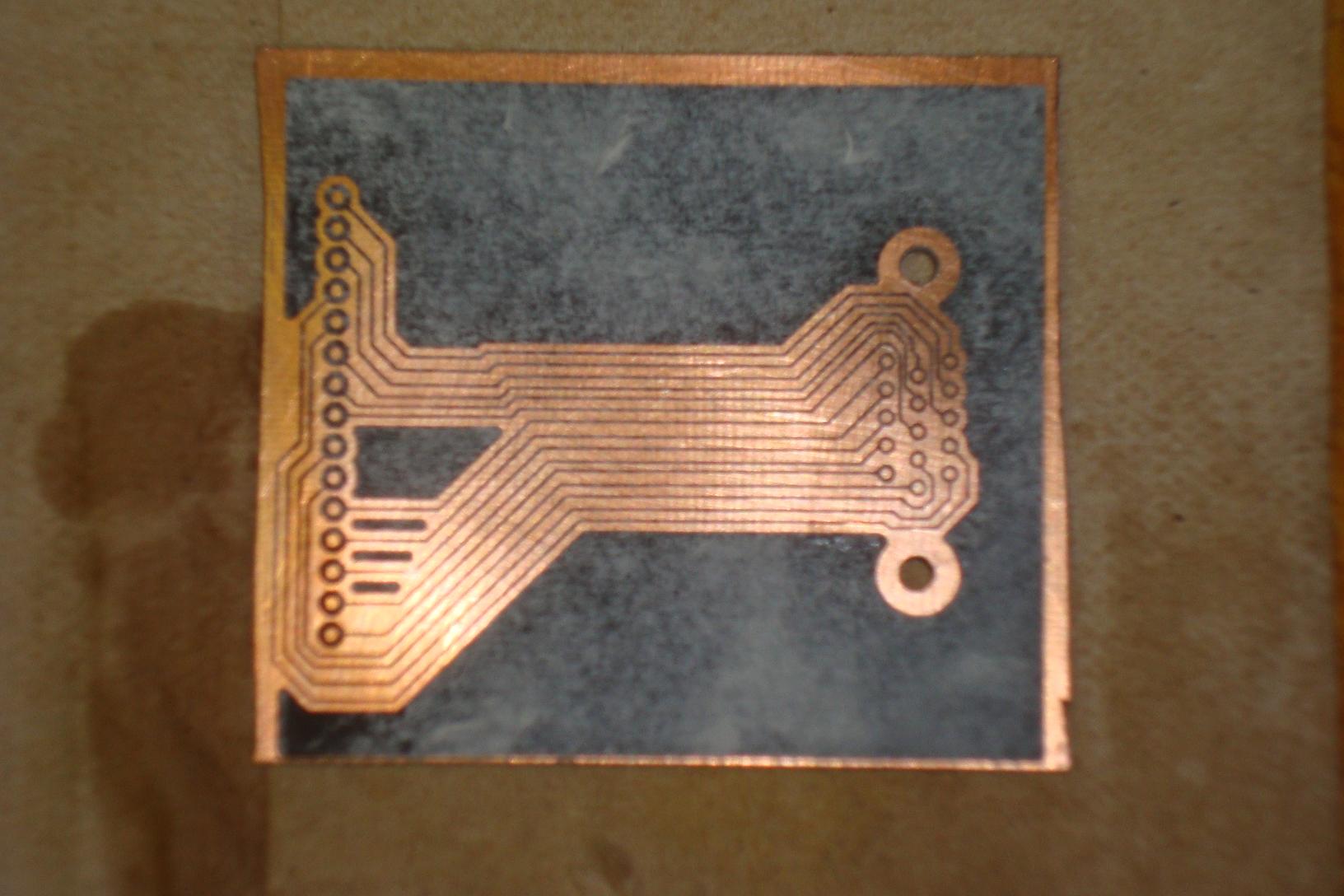
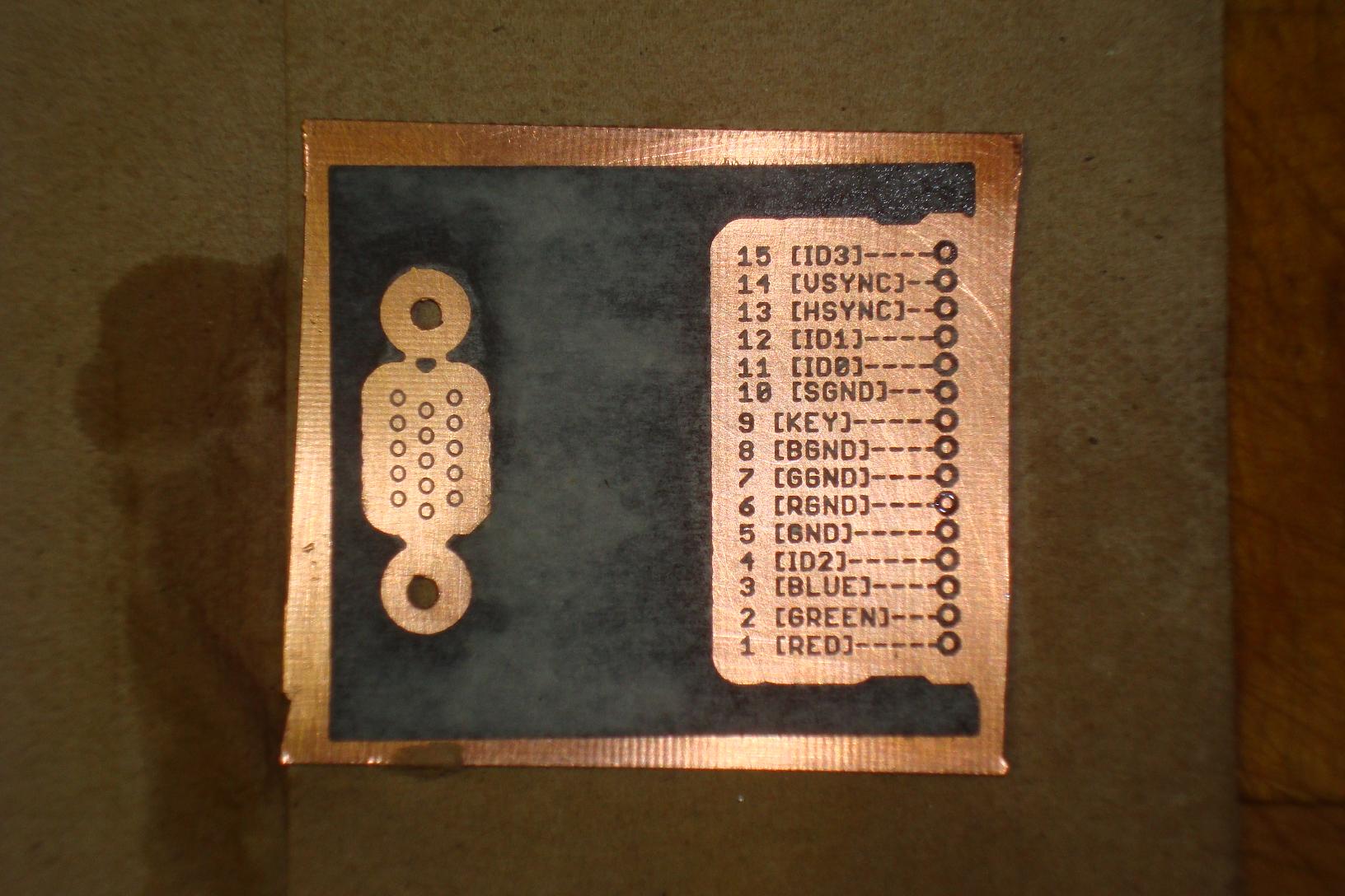
·Throw the board into a bucket of etchant and see how it comes out. You can see below, side A came out looking quite nice.
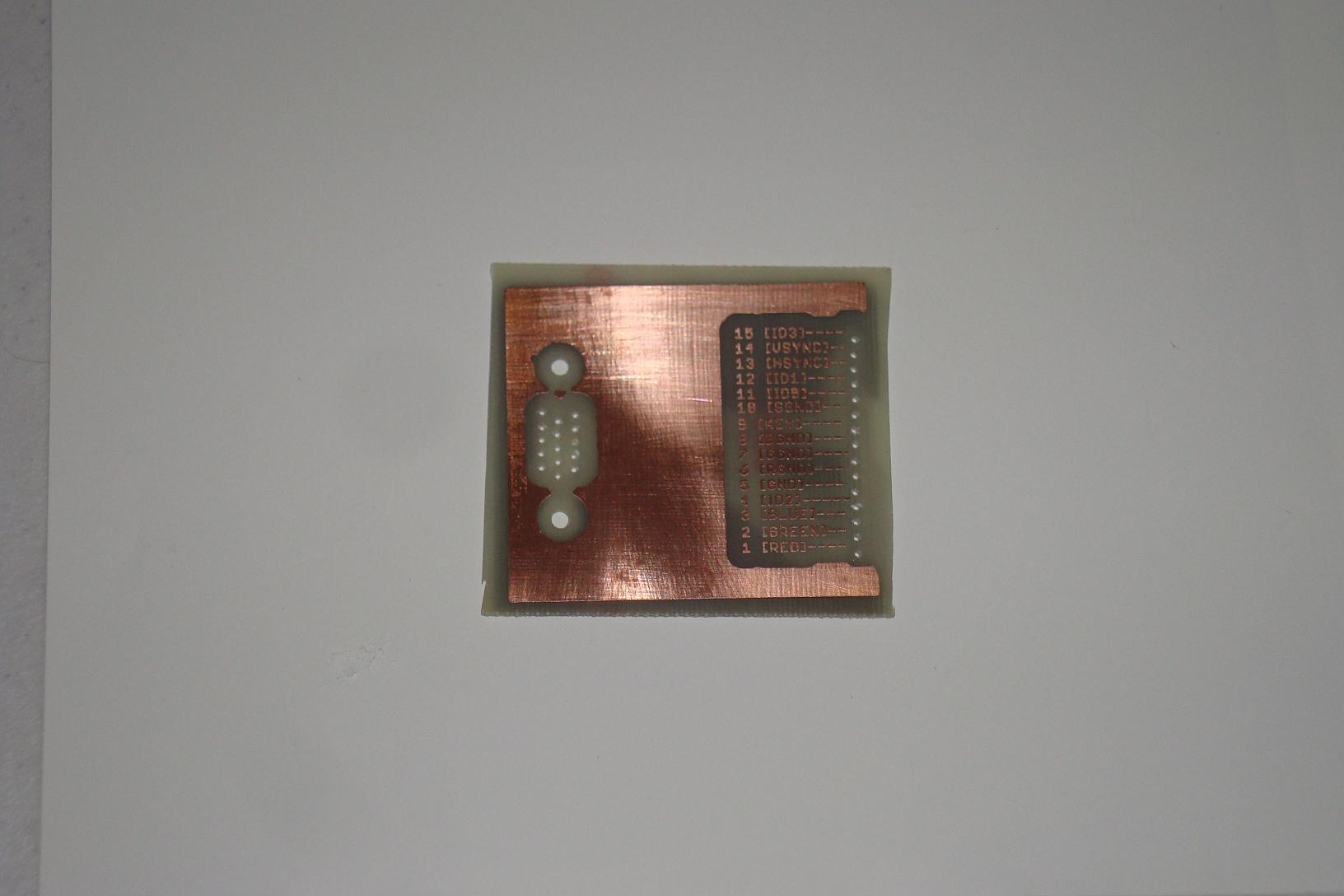
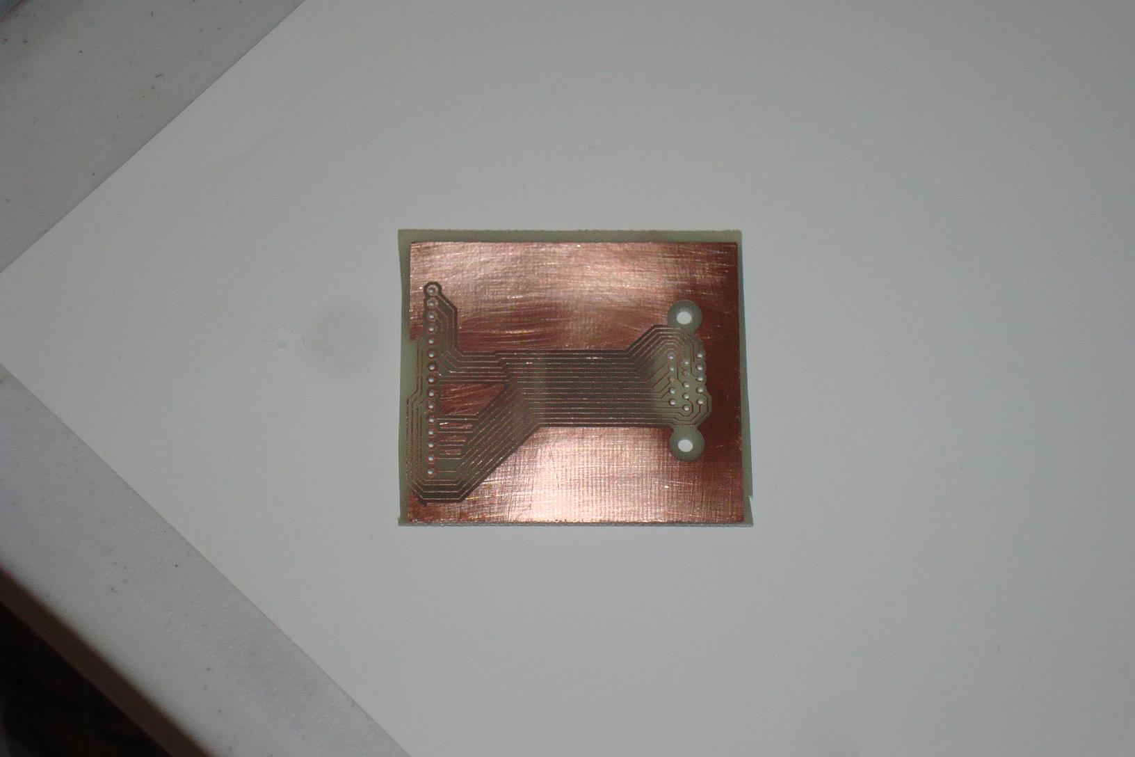
·Side B is also very clean.
·Only two parts need to be soldered into the board.
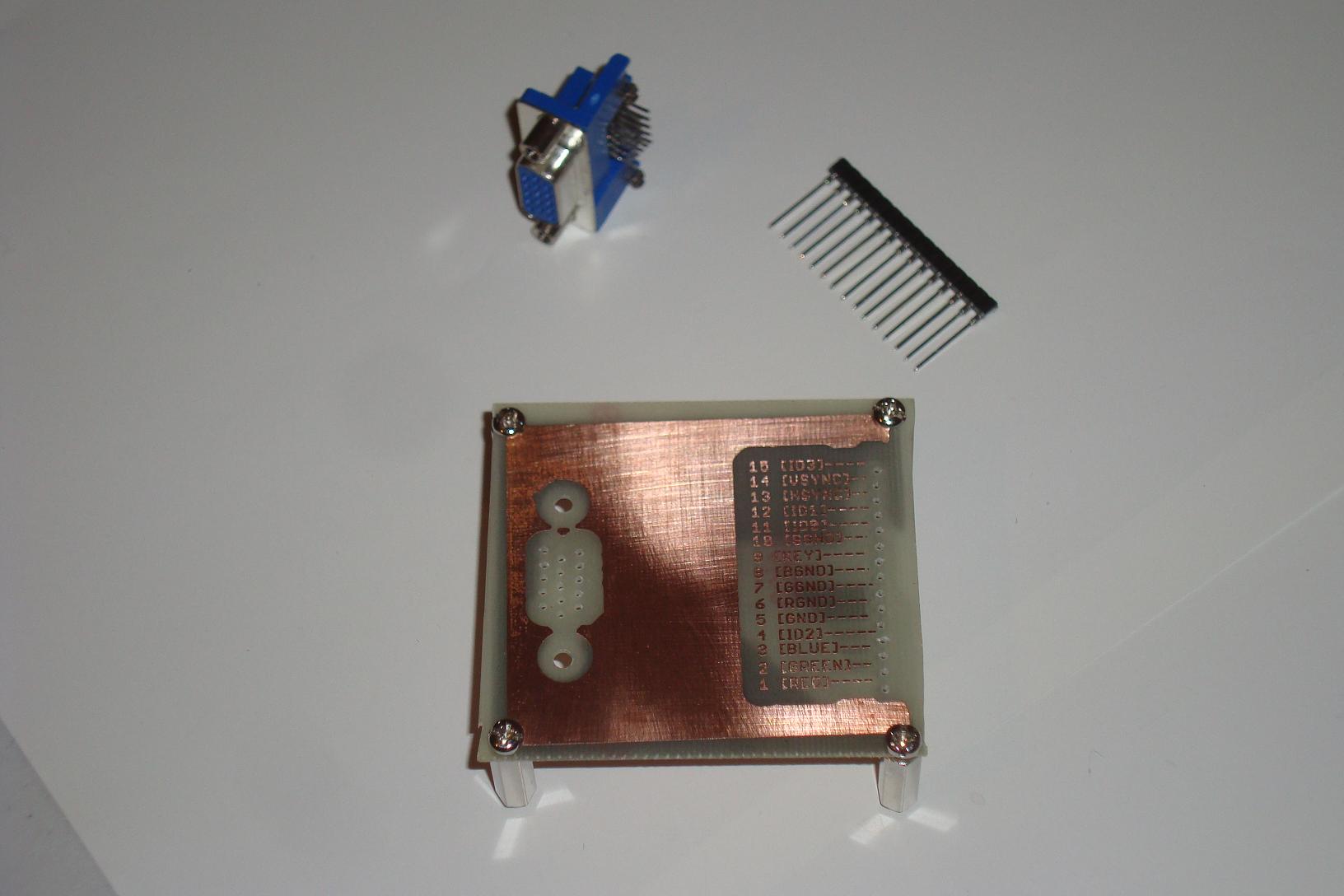
·The VGA connector might take some effort to solder, but the SIPs are easy.
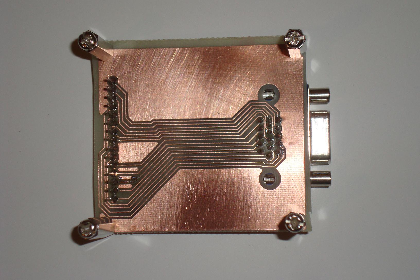
·The board is complete. Use a multimeter's continuity tester to make sure electrical signals make it from connector to connector, through the board.
·All the parts are FINALLY built, let's connect it all together and see how it works and what it does.