Schematic Overview
This schematic is taken directly from the Altera ByteBlaster datasheet or manual. They spill out all the fine print and details of how the connector works & what connections go where. Find the datasheet on their website or through google and give it a good read through.
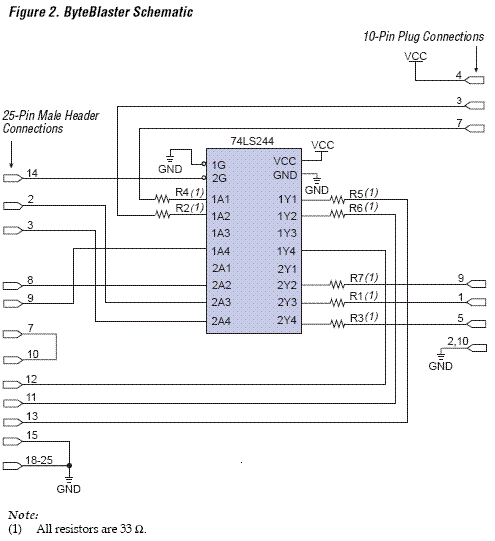
Schematic Specifics
74LS244
The 74LS244 is a Low Power Schottky Octal Buffer. A downside to using this chip in this design is that some computer parallel ports may not offer enough power for this circuit. The ByteBlaster MV is an updated design that solves this problem, something we'll explore later on.
33Ω Resistors
These resisitors act as simple current limiting resistors. They make sure no surge of current can come from the JTAG or Parallel ports that might potentially damage the 74LS244.
DB25 Pins
The pins for the DB25 are all clearly labeled on the left side of the schematic. Notice that not all 25 pins are used.
JTAG 10-Pin Connector
The pins for the 10-Pin connector are again clearly labeled. Notice that only 8 of the 10 pins are actually connected to the JTAG style connector.
This schematic is taken directly from the Altera ByteBlaster datasheet or manual. They spill out all the fine print and details of how the connector works & what connections go where. Find the datasheet on their website or through google and give it a good read through.
Schematic Specifics
74LS244
The 74LS244 is a Low Power Schottky Octal Buffer. A downside to using this chip in this design is that some computer parallel ports may not offer enough power for this circuit. The ByteBlaster MV is an updated design that solves this problem, something we'll explore later on.
33Ω Resistors
These resisitors act as simple current limiting resistors. They make sure no surge of current can come from the JTAG or Parallel ports that might potentially damage the 74LS244.
DB25 Pins
The pins for the DB25 are all clearly labeled on the left side of the schematic. Notice that not all 25 pins are used.
JTAG 10-Pin Connector
The pins for the 10-Pin connector are again clearly labeled. Notice that only 8 of the 10 pins are actually connected to the JTAG style connector.