Hardware Design
The hardware design portion of this project is split into two sections. The first section will take our PCB layout design and build it on an actual PC board. The second section will be devoted to showing you how I assembled the board together with all the parts.
Making The PCB
To make this 2 sided PCB, we will use the toner-transfer process which involves printing the design on glossy paper and ironing it onto the PCB. Follow the pictures below to see how I made the PCB using the eagle design seen on the schematic page.

First, the top and bottom layers of the design are printed out on glossy paper from a laser printer.

Using a hot iron, the top and bottom layers' toner is transferred by 'ironing' the design onto the copper on the PCB.
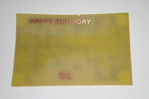
The result is that the toner is now on the PCB and as you can see the circuit above.....
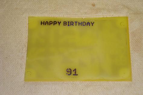
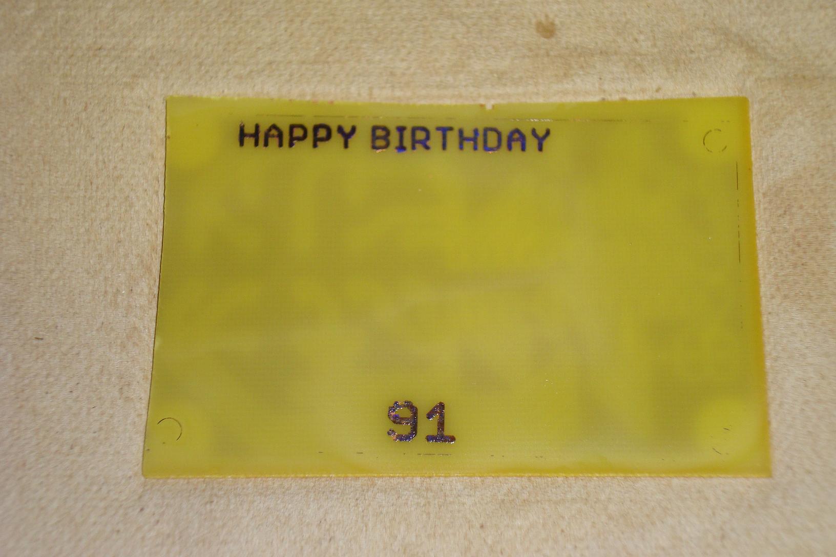
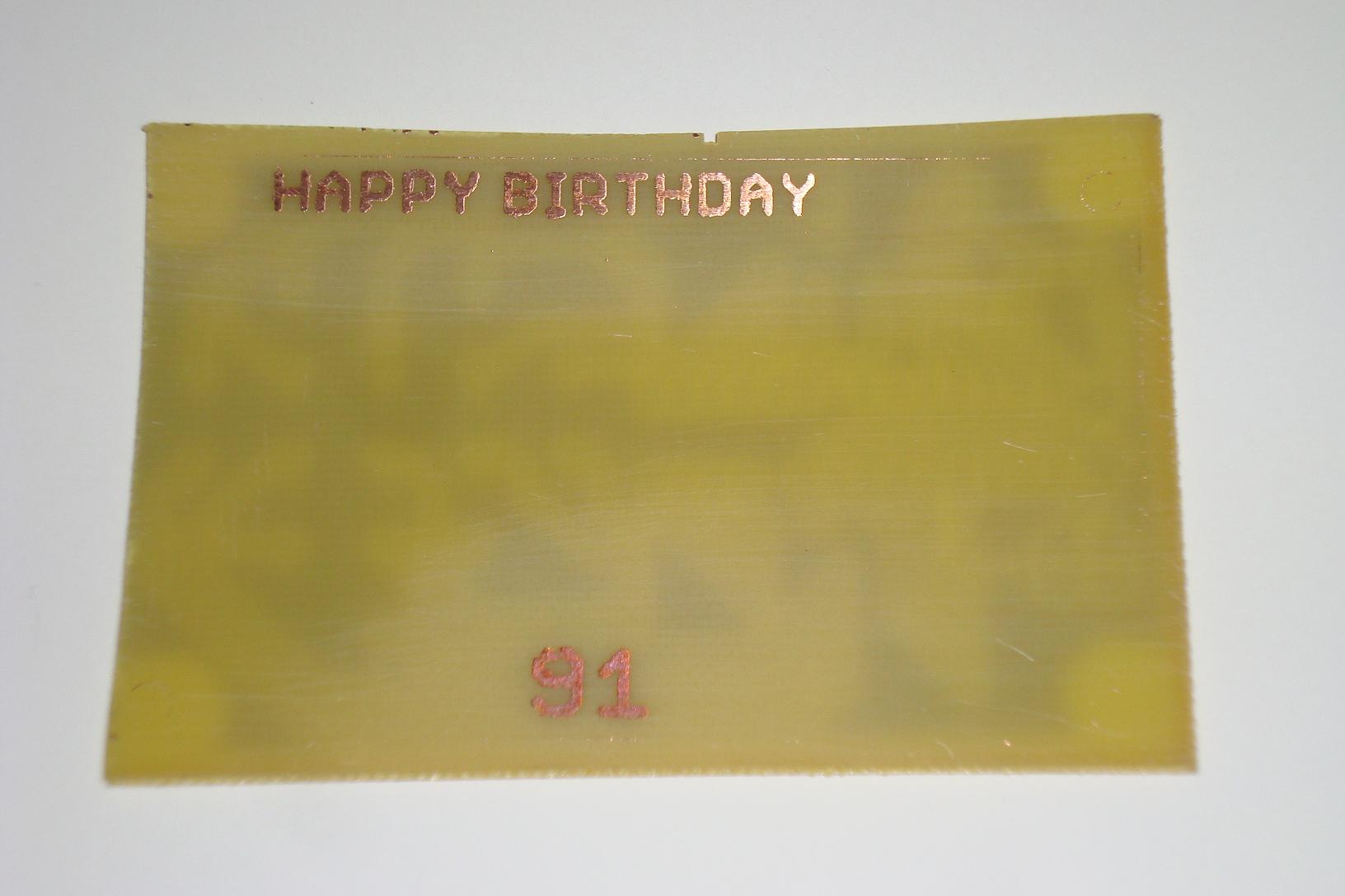
And the top side which will have most of it's copper etched away, leaving only the short message behind.
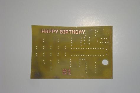
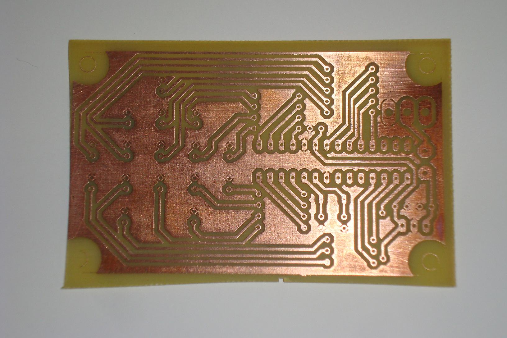
After etching the board, you can see the copper has been eaten away except for where the toner was.
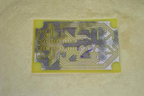
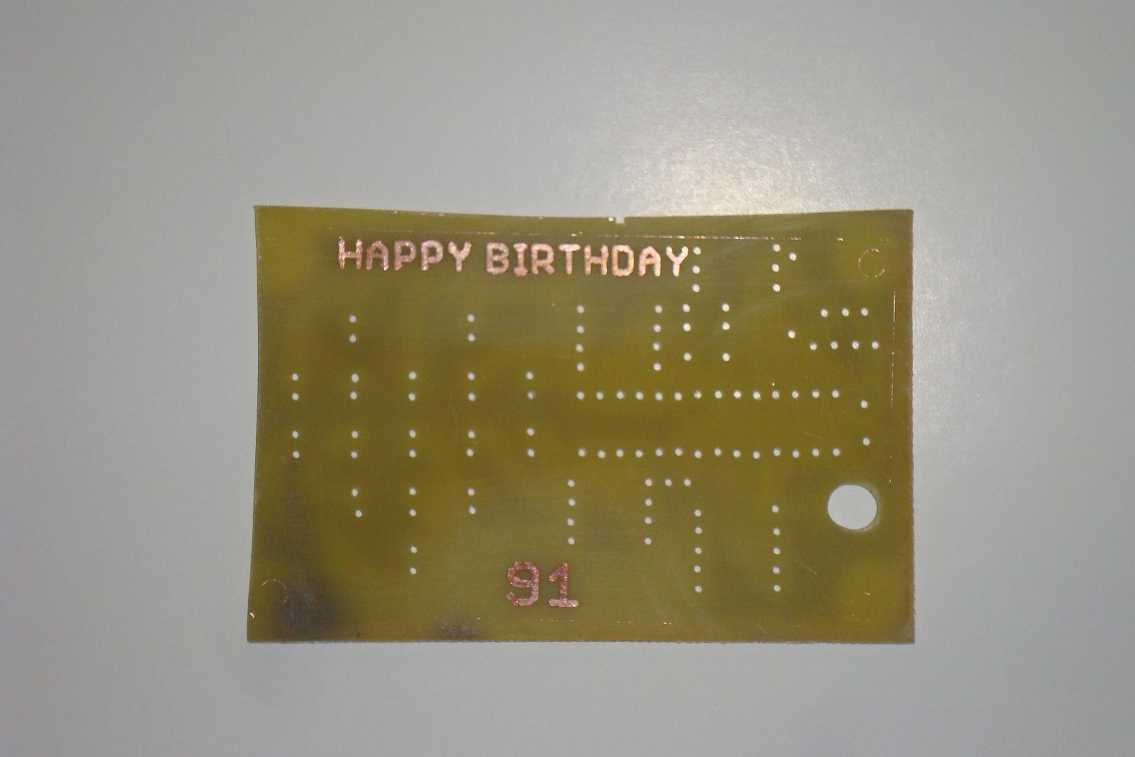
Similarly, on the bottom of the board all of the copper is etched away leaving only the toner covered portion.

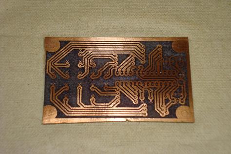
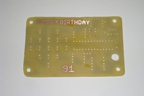
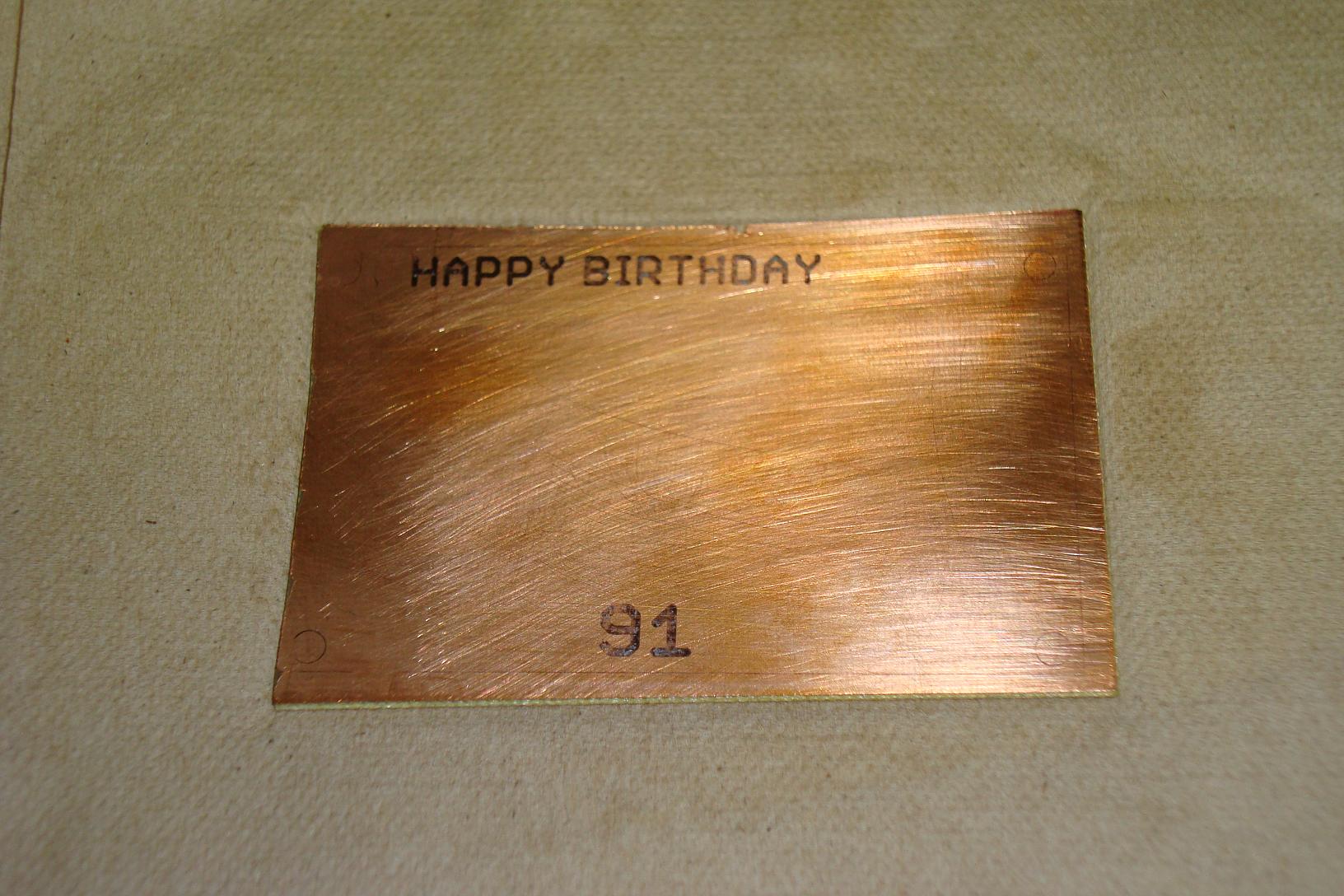
Scratching off the toner, you can better see how the copper was protected and our circuit is now on the PCB.
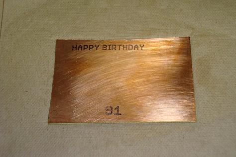
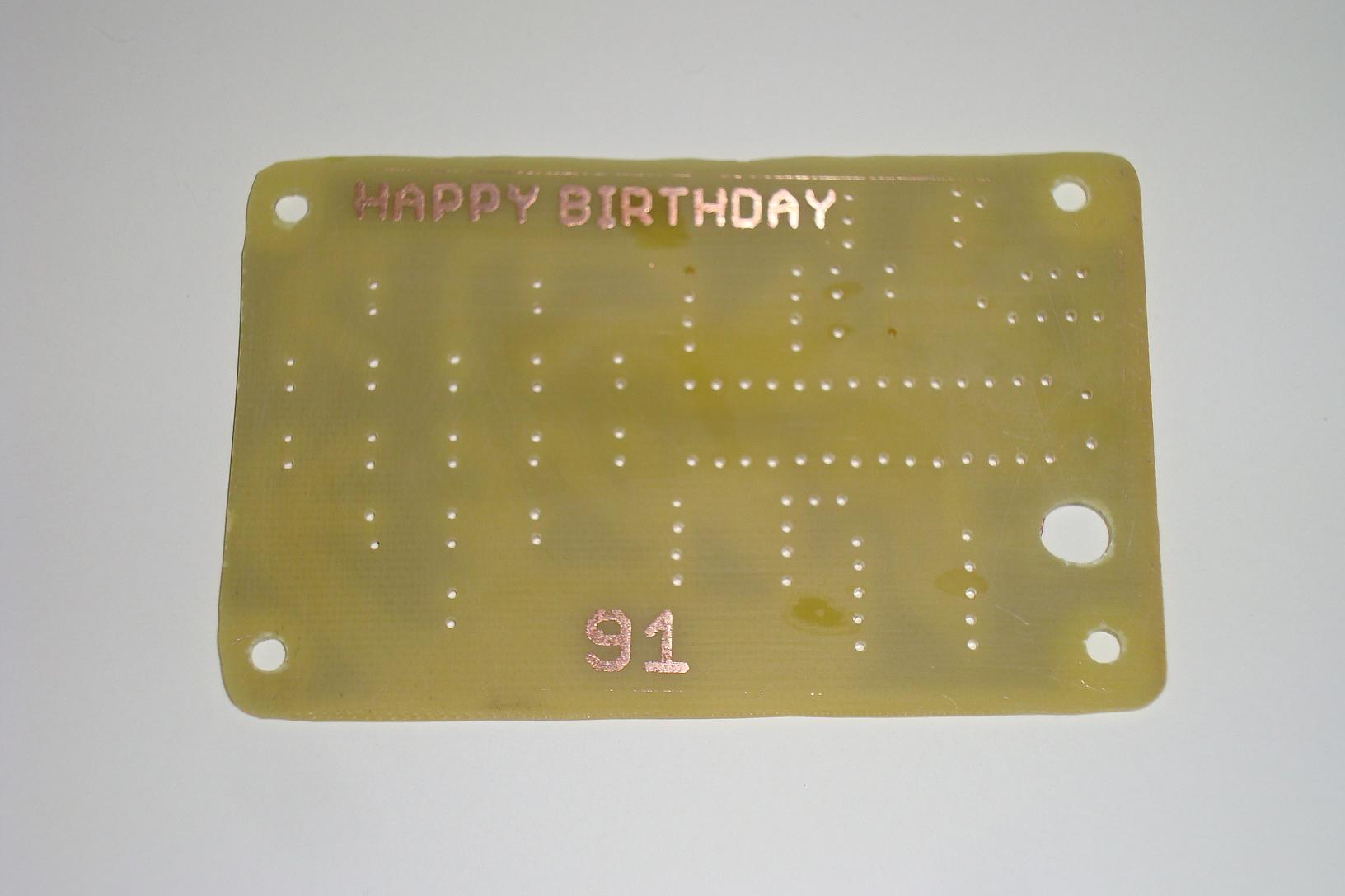
The top side also looks nicer after we scratch off the toner and leave only the copper on the board.
Hopefully you have a drill press. If not, a standard power drill will work to get all the holes into the board.
After getting the holes into the board, if you have a sander or any means to round the edges, it makes the PCB far more user friendly and won't scratch anybody.
The hardware design portion of this project is split into two sections. The first section will take our PCB layout design and build it on an actual PC board. The second section will be devoted to showing you how I assembled the board together with all the parts.
Making The PCB
To make this 2 sided PCB, we will use the toner-transfer process which involves printing the design on glossy paper and ironing it onto the PCB. Follow the pictures below to see how I made the PCB using the eagle design seen on the schematic page.
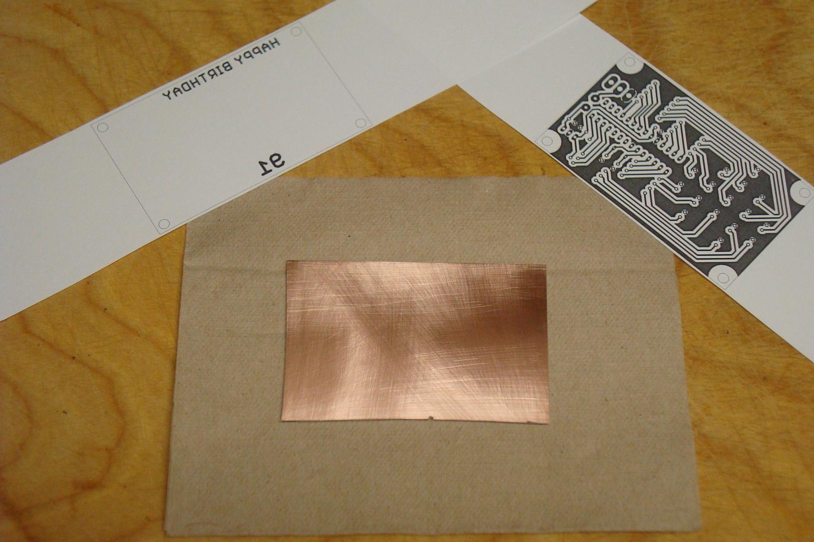
First, the top and bottom layers of the design are printed out on glossy paper from a laser printer.
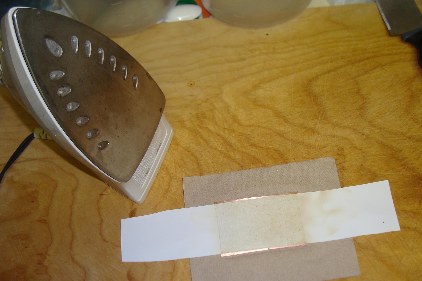
Using a hot iron, the top and bottom layers' toner is transferred by 'ironing' the design onto the copper on the PCB.

The result is that the toner is now on the PCB and as you can see the circuit above.....
And the top side which will have most of it's copper etched away, leaving only the short message behind.
After etching the board, you can see the copper has been eaten away except for where the toner was.
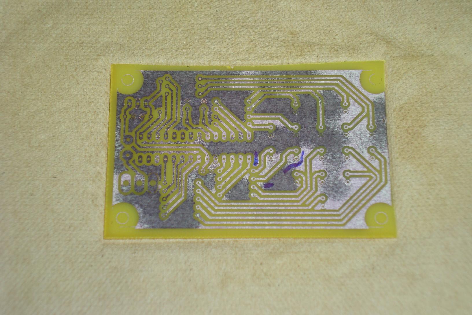
Similarly, on the bottom of the board all of the copper is etched away leaving only the toner covered portion.
Scratching off the toner, you can better see how the copper was protected and our circuit is now on the PCB.
The top side also looks nicer after we scratch off the toner and leave only the copper on the board.
Hopefully you have a drill press. If not, a standard power drill will work to get all the holes into the board.
After getting the holes into the board, if you have a sander or any means to round the edges, it makes the PCB far more user friendly and won't scratch anybody.