Schematic Overview
The great thing about these little Xbee modules is they take care of almost all the heavy lifting. As you can see below both the transmitter and the receiver circuits are drop-dead simple. The main devices used in the circuit are the Xbee Modules, PIC 18LF452 and LM317.
Transmitter Schematic
View Full Schematic
Receiver Schematic
View Full Schematic
Schematic Specifics
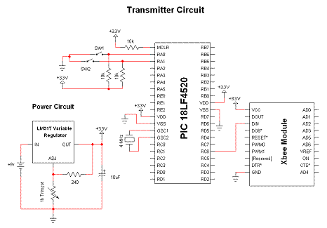
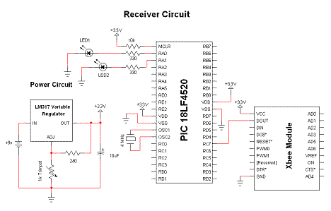
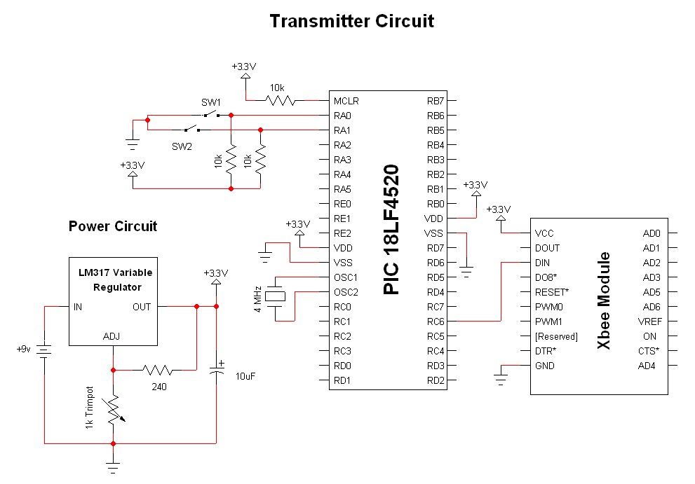
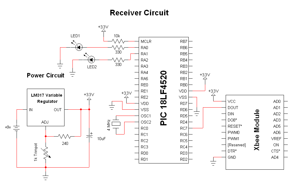
Power Circuit
Both circuits use the same simple power regulation circuit with the LM317 for +3.3v reg. An output capacitor of 10uF is used for noise filtering which helps keeps the output DC signal stable around +3.3v. A 1k or 5k trimmer is used with a 240ohm resistor to create the adjustable voltage to the required +3.3v
Transmitter Circuit
The transmitter circuit has the standard PIC 18LF4520 power, ground, MCLR and crystal connections. In addition to the normal connections, two buttons are connected to PORTA pins 0 and 1. A pull up resistor of 10kΩ is used so that the digital input seen is +5v or logic 1. When either button is pressed, the input is connected to ground/+0v making the input a logic 0. PortB pin 0 is connected to the Xbee Din pin. This is for the wireless data to be output to the receiver.
Receiver Circuit
The receiver circuit has the same standard PIC power, ground, MCLR and crystal connections. The difference between the transmitter is instead of input via buttons, we are showing output with an LED. Similarly, the PORTB pin 0 is connected to the Dout pin of the Xbee module so that the wirelessly transmitted information can be received.
The great thing about these little Xbee modules is they take care of almost all the heavy lifting. As you can see below both the transmitter and the receiver circuits are drop-dead simple. The main devices used in the circuit are the Xbee Modules, PIC 18LF452 and LM317.
View Full Schematic
View Full Schematic
Schematic Specifics
Power Circuit
Both circuits use the same simple power regulation circuit with the LM317 for +3.3v reg. An output capacitor of 10uF is used for noise filtering which helps keeps the output DC signal stable around +3.3v. A 1k or 5k trimmer is used with a 240ohm resistor to create the adjustable voltage to the required +3.3v
Transmitter Circuit
The transmitter circuit has the standard PIC 18LF4520 power, ground, MCLR and crystal connections. In addition to the normal connections, two buttons are connected to PORTA pins 0 and 1. A pull up resistor of 10kΩ is used so that the digital input seen is +5v or logic 1. When either button is pressed, the input is connected to ground/+0v making the input a logic 0. PortB pin 0 is connected to the Xbee Din pin. This is for the wireless data to be output to the receiver.
Receiver Circuit
The receiver circuit has the same standard PIC power, ground, MCLR and crystal connections. The difference between the transmitter is instead of input via buttons, we are showing output with an LED. Similarly, the PORTB pin 0 is connected to the Dout pin of the Xbee module so that the wirelessly transmitted information can be received.