Schematic Overview
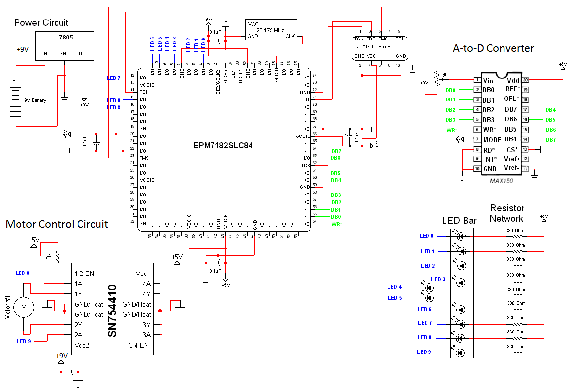
An issue with CPLD and FPGA devices is that they have so many I/O pins that their schematics become overwhemlingly HUGE very quickly. I tried my best to partition out different sections of the schematic to show the motor control circuit, a-to-d converter circuit and left-over LED output circuit.

View Full Schematic
Schematic Specifics
Motor Control Circuit
The motor control circuit is the main focus as it is the new addition to this board. As you can see in the schematic, we're basically wiring things up to power, ground and 2 wires go to the CPLD. A capacitor is added near the motor controller IC to make sure that it can provide a steady flow of current to the motors.
A-To-D Converter Circuit
This circuit is unchanged from the CPLD A-to-D article. The MAX150 is in a constantly converting mode whenever the WR pin is asserted it updates. The CPLD takes care of this for us.
LED Output Circuit
This circuit is also left over from the previous article, but I feel it makes a great addition as we can output the PWM signal to the LEDs as well as to the motor controller, this way we can really see the direction/speed control in two forms: in motor movement and in LED's brightness.
An issue with CPLD and FPGA devices is that they have so many I/O pins that their schematics become overwhemlingly HUGE very quickly. I tried my best to partition out different sections of the schematic to show the motor control circuit, a-to-d converter circuit and left-over LED output circuit.
View Full Schematic
Schematic Specifics
Motor Control Circuit
The motor control circuit is the main focus as it is the new addition to this board. As you can see in the schematic, we're basically wiring things up to power, ground and 2 wires go to the CPLD. A capacitor is added near the motor controller IC to make sure that it can provide a steady flow of current to the motors.
A-To-D Converter Circuit
This circuit is unchanged from the CPLD A-to-D article. The MAX150 is in a constantly converting mode whenever the WR pin is asserted it updates. The CPLD takes care of this for us.
LED Output Circuit
This circuit is also left over from the previous article, but I feel it makes a great addition as we can output the PWM signal to the LEDs as well as to the motor controller, this way we can really see the direction/speed control in two forms: in motor movement and in LED's brightness.