Schematic Overview
The schematic for this project is a modified version of the CPLD dev board schematic. There are a few new parts added for this project and you can see the completed schematic for this project below. The main parts in the schematic are the CPLD Dev Board, MAX233a and 7 Segment Display.
EPM7128 CPLD + MAX233A Interface
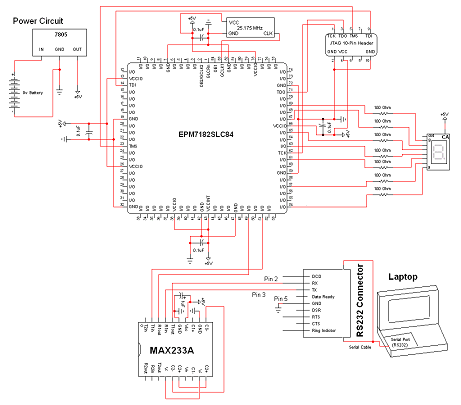
View Full Schematic
Schematic Specifics
Power Regulator
The power regulation circuit is a LM7805 +5v regulator that will convert the +9v from the battery to a steady +5v output to the CPLD.
MAX233A Circuit
The RS232 interface circuit consists of the CPLD, it's 25.175 MHz crystal clock and the MAX233A. The MAX233A translates the +12v higher voltage RS232 signals into TTL +5v logic that the FPGA can understand.
CPLD Dev Board
This protoboard for a cpld was developed by me a few years ago. It's really just a PLCC CPLD in a socket with power and JTAG connectors for programming.
25.175 MHz Oscillator
This oscillator was chosen mostly at random. We needed some type of timing device to keep a reference to time and I had this one laying around. Generally if you can find a clock above 10 MHz you'll be fine for this project.
The schematic for this project is a modified version of the CPLD dev board schematic. There are a few new parts added for this project and you can see the completed schematic for this project below. The main parts in the schematic are the CPLD Dev Board, MAX233a and 7 Segment Display.
EPM7128 CPLD + MAX233A Interface
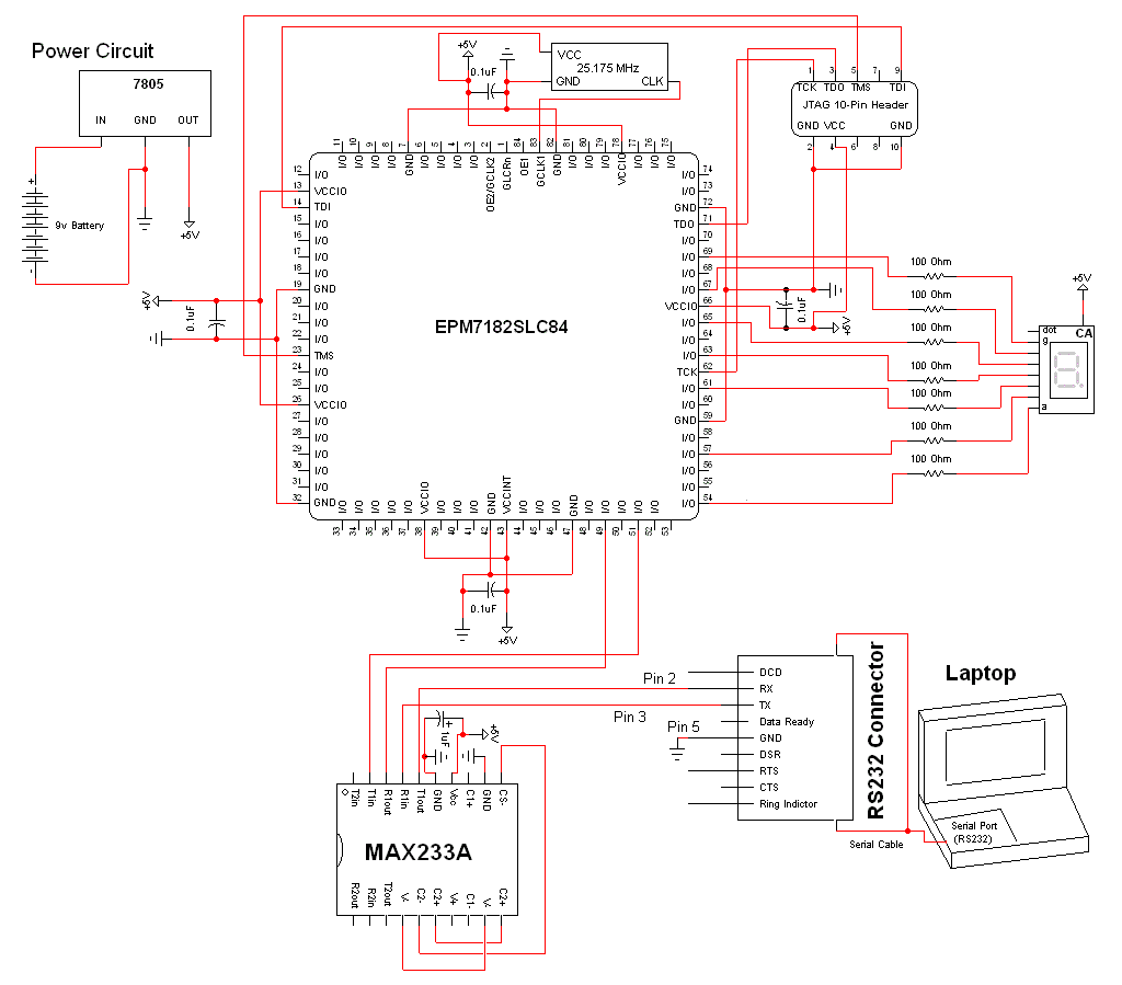
View Full Schematic
Schematic Specifics
Power Regulator
The power regulation circuit is a LM7805 +5v regulator that will convert the +9v from the battery to a steady +5v output to the CPLD.
MAX233A Circuit
The RS232 interface circuit consists of the CPLD, it's 25.175 MHz crystal clock and the MAX233A. The MAX233A translates the +12v higher voltage RS232 signals into TTL +5v logic that the FPGA can understand.
CPLD Dev Board
This protoboard for a cpld was developed by me a few years ago. It's really just a PLCC CPLD in a socket with power and JTAG connectors for programming.
25.175 MHz Oscillator
This oscillator was chosen mostly at random. We needed some type of timing device to keep a reference to time and I had this one laying around. Generally if you can find a clock above 10 MHz you'll be fine for this project.